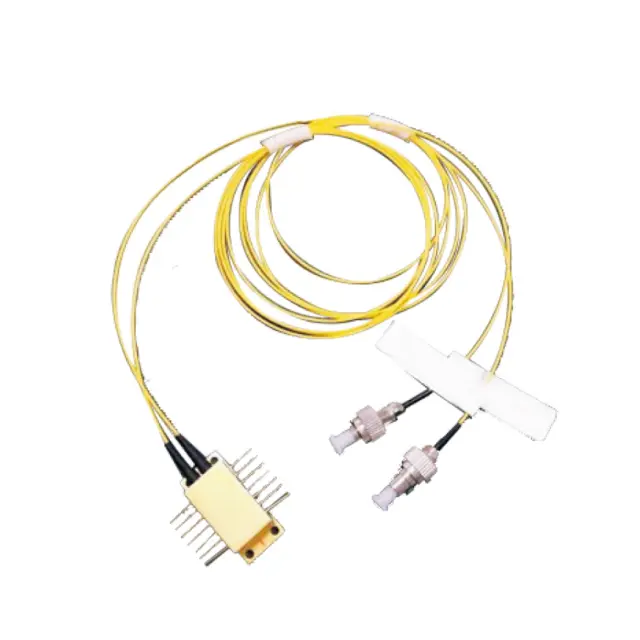


-Working wavelength:0.95μm~1.65μm;
-Designed for single photon detection applications;
-Internal integrated three-stage TEC cooler;
-Butterfly hermetically sealed dual channel module with pigtail.
Linear mode parameters
| Characteristic Parameters | Test conditions(TC=25±5℃ unless otherwise Specified) | Minimal | Greatest | Unit |
| Effective detection surface diameter d | – | 25 | – | μm |
| Spectral Response Range | – | 950 | 1650 | nm |
| Reverse breakdown voltage V\(_{BR}\) | I\(_{R}\) =10 μA, Φe=0 | 60 | 85 | V |
| Responsiveness R\(_{e}\) | Φ\(_{e}\) =1μW, VR=(V\(_{BR}\) -1)V, λ=1550 nm±50 nm | 8 | – | A/W |
| Dark Current I\(_{D}\) | VDC=(V\(_{BR}\) -1)V, Φe=0 | – | 1 | nA |
| Capacitance C\(_{tot}\) | VDC=(V\(_{BR}\) -1)V, f=1MHz | – | 0.2 | pF |
| Temperature coefficient of | T\(_{C}\) =-45~+30℃,I\(_{R}\) =10μA, φe=0 | 0.10 | 0.2 | V/℃ |
| breakdown voltage η |
Geiger model parameters
| Characteristic Parameters | Test conditions(TC=25±5℃ unless otherwise specified) | Minimal | Greatest | Unit |
| Single Photon Detection Efficiency PDE | TA=-40±5℃,μ=1,fg=1.0 GHz, fp=500 kHz,DCR≤2.5 kHz,λ=1.55 μm | 3 | – | % |
| Dark Count Rate DCR | TA=-40±5℃,fg=1.0 GHz. | – | 2.5 | kHz |
| SPDE =20%,λ=1.55μm | ||||
| Post-Pulse Probability APP (500 ns) | TA=-40±5℃,μ=1,fg=1.0 GHz,fp=500 kHz. DCR≤3.0 kHz,SPDE =10%,λ=1.55 μm | – | 4 | % |
| Time Jitter T\(_{J}\) | SPDE=10% | – | 300 | ps |
| Note: λ is the wavelength o incident light,T\(_{A}\) is the value of testtemperature ,μ is the average number of photons per pulse,fg is the frequency of gating signal and fp is the frequency of optical pulse signal. | ||||
| Absolutely Maximum rating | 1 | Storage temperature T\(_{STG}\) | -50℃~+85℃ |
| 2 | Operating ambient temperature T\(_{C}\) | -50℃~60℃ | |
| 3 | Welding temperature T\(_{sld}\) (time) | 260℃(10s) | |
| 4 | Reverse DC bias voltage \(_{VDC}\) | VB+5V | |
| 5 | Input optical power φe(continuous) | 1mW | |
| 6 | Forward current I\(_{F}\) (continuous) | 200μA | |
| 7 | Electrostatic Discharge Sensitivity ESD | ≥300V | |
| 8 | Pigtail Tension | 3.0N | |
| 9 | TEC Voltage | 11.9 V | |
| 10 | TEC Current | 0.8 A |
| Serial Number | Parameters | Rated Value | |
| Recomm endation | 1 | APD chip operating temperature T\(_{th}\) | -50℃~-30℃ |
| Referral working | 2 | Reverse DC bias voltage V\(_{DC}\) | V\(_{BR}\) + 1V to V\(_{BR}\)+5V |
| conditions | |||
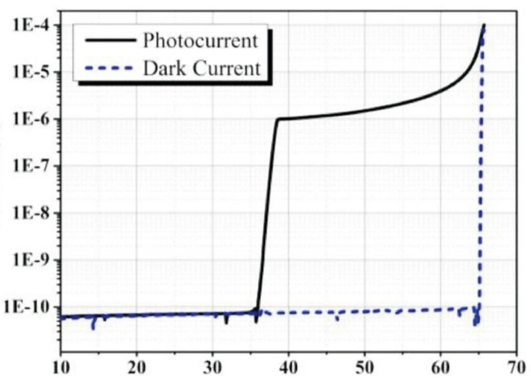
Voltage(V)
Fig.1 Photocurrent and dark current curves
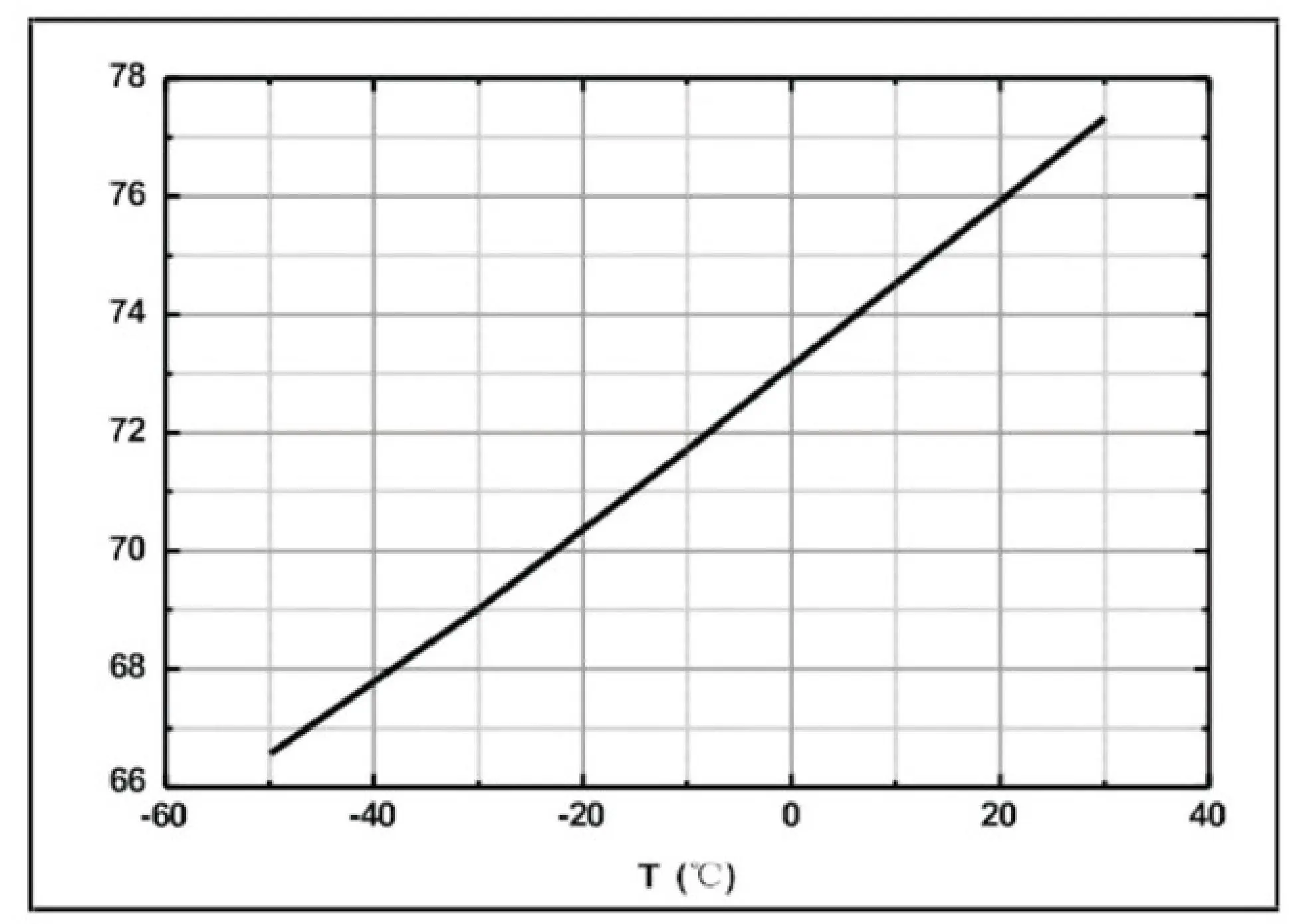
Fig.2 Temperature coefficient of breakdown voltage

Figure 3 Product form factor
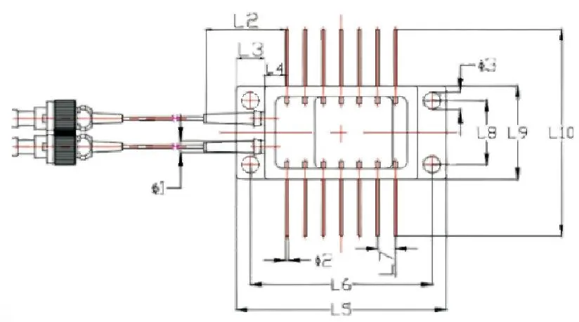
The external dimensions of the product are shown in Table 2.
| nominal value | maximum value | notation | minimum value | nominal value | maximum value | notation | minimum value | nominal value | maximum value |
| – | 7.0 | L2 | 10.0 | – | 30.0 | L8 | 8.8 | – | 9.2 |
| – | 2.2 | L3 | 3.8 | – | 4.2 | L9 | 12.5 | – | 13.5 |
| – | 7 | L4 | 3 | – | 3.3 | L10 | 28.5 | – | 30.5 |
| – | 10.5 | L5 | 29.2 | – | 29.8 | ф1 | 3 | – | 6.6 |
| – | – | L6 | 24.5 | – | 25.5 | ф2 | 0.35 | – | 0.5 |
| – | 21.8 | L7 | – | 2.54 | – | ф3 | 2.2 | – | 2.6 |
Output Port Definitions
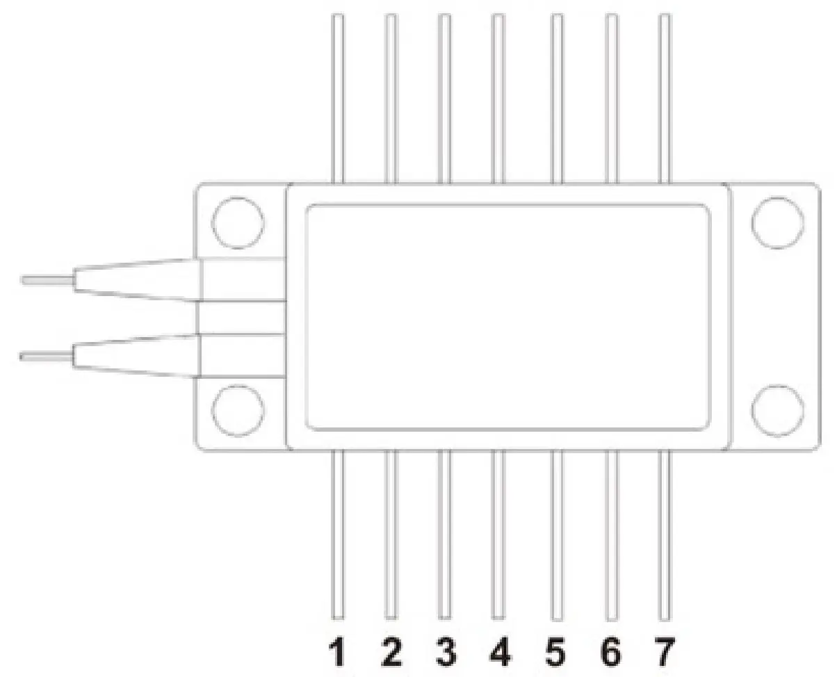
Fig.4 Pin arrangement and numbering (top view)
| Outlet Numbering | Name (symbol) | Outlet Numbering | name (of a thing) | |
| 1 | reserve | 8 | reserve | |
| 2 | reserve | 9 | reserve | |
| 3 | Diode I(N-pole) | 10 | Diode Il (N-pole) | |
| 4 | Diode I signal output (Vout) | 11 | Diode ll signal output (V\(_{out}\)) | |
| 5 | Diode I(P-pole) | 12 | Diode ll(P-pole) | |
| 6 | Thermistor (Rth) | 13 | Thermistor(Rth) | |
| 7 | Chiller Positive(TEC+) | 14 | Chiller Positive(TEC-) | |
| TEC\NTC Electrical Parameters NTC (Temperature Sensitive Resistor):R\(_{T}\)=10kΩ@25℃,β=3450,5 %. TEC (temperature difference cooler):I\(_{MAX}\)=0.8A,V\(_{MAX}\)=11.9 V,T\(_{HMAX}\)=200℃ . | ||||
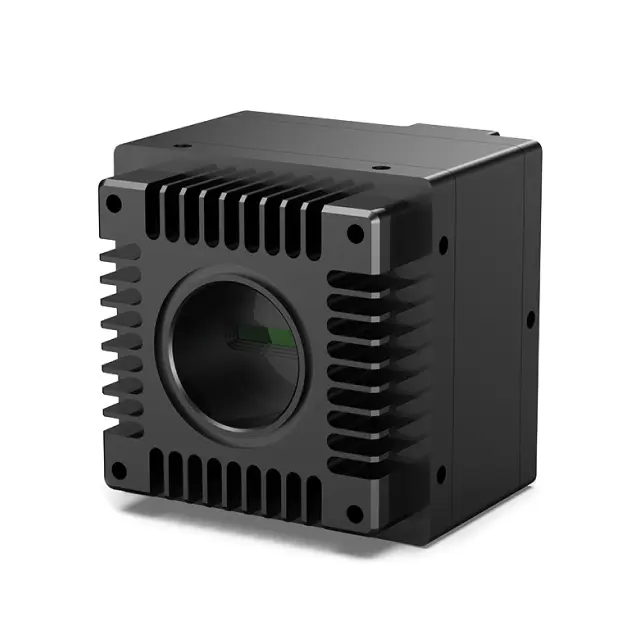
Visible Light⁺ Near-Infrared Camera
This camera is suitable for the spectral range of 400-1700nm, covering the visible light to shortwave
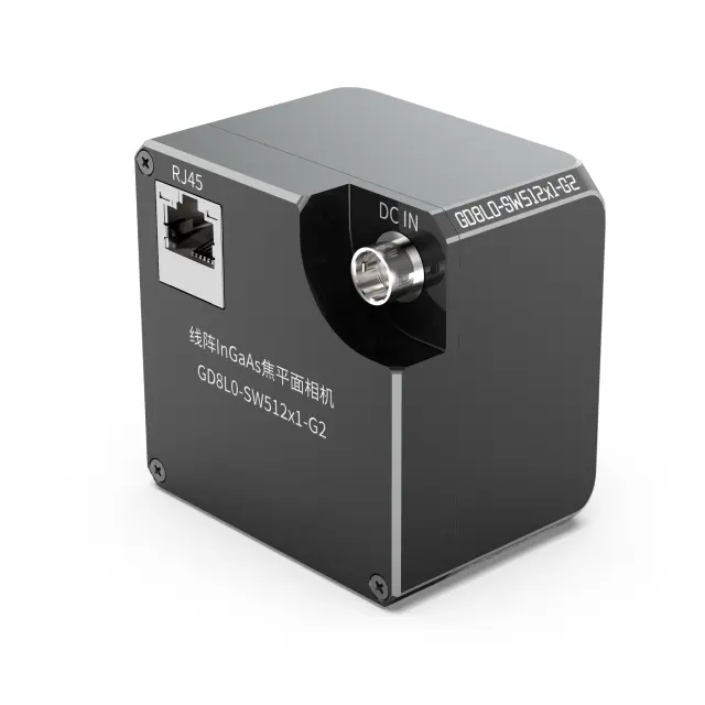
InGaAs Linear Focal Plane Camera
The industrial grade linear array shortwave infrared camera is designed for the spectral ange of 900-1700nm
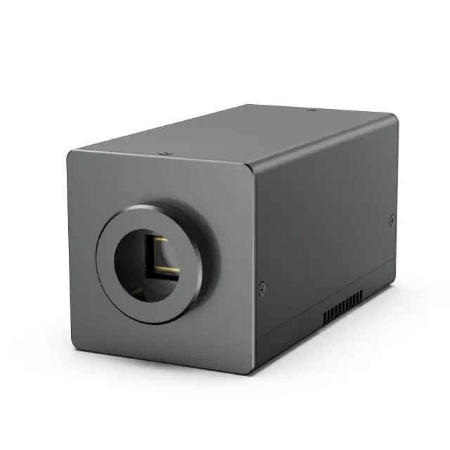
InGaAs Face Array Focal Plane Camera
This product uses domestically produced high sensitivity InGaAs array detectors, with array sizes of 320×256
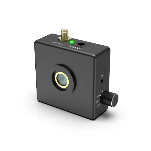
InGaAs Avalanche Photon Detector
This product is a compact near-infrared avalanche photodetector with a core circuit made of domestically
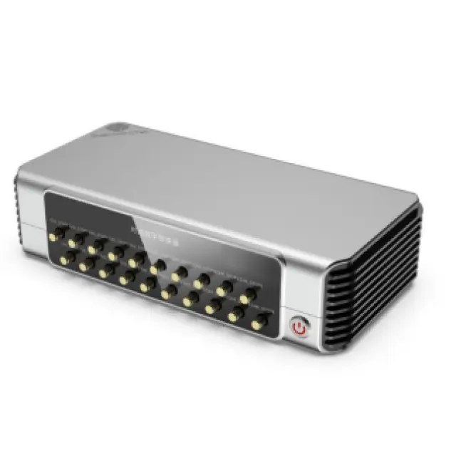
Time-to-Digital Converter
The QTDC-16CH-0A is a compact, high-precision measurement instrument featuring 16 acquisition
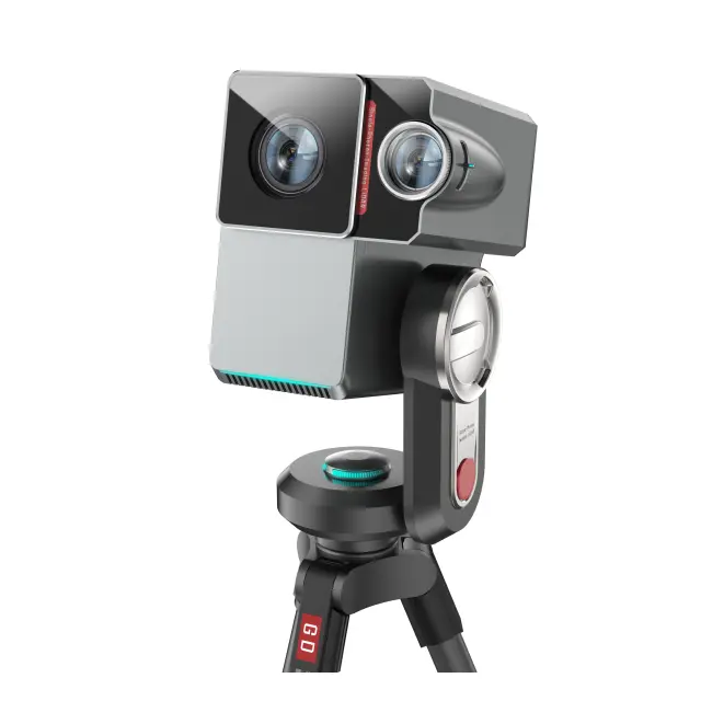
Single Photon Ranging System
This product adopts a fiber optic coaxial optical path design and an integrated system design,which has good stability