


Understanding Near-Infrared Cameras: Basics for Engineers
Near-infrared (NIR) cameras are optical imaging devices designed to detect light just beyond the visible spectrum — typically between 750 nm and 1700 nm. This spectral region is invisible to the human eye but contains critical information for material identification, moisture content detection, and subsurface inspection.
There are two major regions in the infrared spectrum relevant to imaging:
- NIR / SWIR (Short-Wave Infrared): ~0.75 μm to 1.7 μm
- MWIR & LWIR: Longer wavelengths (used in thermal cameras)
NIR cameras generally use InGaAs (Indium Gallium Arsenide) sensors, which are highly sensitive in the 900–1700 nm range. However, standard InGaAs sensors do not detect visible light, which limits versatility. That’s where dual-band sensors (Si + InGaAs) come in — they combine the visible (400–700 nm) with SWIR (900–1700 nm) in a single device. This makes them ideal for multispectral imaging without needing two separate cameras.
In industrial and scientific contexts, NIR imaging reveals features that are:
- Invisible to RGB sensors (e.g., internal bruising in fruit, cracks in silicon)
- Sensitive to chemical composition, water absorption, or thermal effects
- Often used in semiconductor, agriculture, recycling, solar cell, and coating thickness inspection
Visible and Near-Infrared Imaging (400–1700 nm) with Si+InGaAs Sensors
Capturing images across visible and short-wave infrared (SWIR) wavelengths requires combining different detector materials, since traditional silicon-based sensors rapidly lose sensitivity beyond ~950 nm. The 400–1700 nm spectral range of the GD9L0-130CN-G2 / GD9L0-33CN-G2 camera covers the full visible band and the SWIR region, bridging this gap. It achieves this via a Si+InGaAs dual-sensor design (integrating a silicon photodiode array with an InGaAs array) that enables broad-band imaging in one device. In the visible range (approximately 400–700 nm) silicon excels with high quantum efficiency, while the InGaAs portion detects longer wavelengths up to 1.7 μm that silicon can’t capture. By unifying these technologies, the camera can reveal features invisible to conventional visible-light cameras – for example, moisture or silicon material variations that only appear under SWIR illumination – while still imaging normal visible details. This dual-band approach provides a more complete picture in inspection tasks, eliminating the need for two separate camera systems to cover the different spectra.
Key Features and Specifications of the GD9L0 Series Cameras
The GD9L0-130CN-G2 and GD9L0-33CN-G2 are high-performance industrial cameras that offer dual-band spectral imaging alongside advanced on-board processing and robust design. Below are their notable technical features:
- Dual-Band Imaging (0.4–1.7 μm): Both models use Si+InGaAs sensor arrays to simultaneously capture visible through SWIR wavelengths, delivering imaging across a broad 400–1700 nm spectrum. This allows one camera to detect standard visible features as well as SWIR-specific details (e.g. water content or silicon penetration) in real time. The sensor arrays have a 5 μm × 5 μm pixel pitch and come in two resolution options: 1280 × 1024 (≈1.3 MP) and **640 × 512 (≈0.33 MP)**.
- Resolution and Frame Rates: The 1.3 MP model (GD9L0-130CN-G2) delivers up to 1280×1024 at 38 frames per second, while the 0.33 MP model (GD9L0-33CN-G2) can reach 640×512 at 152 fps for high-speed imaging. Both sensors use a global shutter exposure (7 μs minimum shutter, up to 0.1 s) so that fast motion is frozen without distortion. The camera outputs 8-bit, 10-bit or 12-bit monochrome images, providing flexibility in dynamic range versus data size.
- High Dynamic Range and Low Noise: The dual-band sensor achieves a dynamic range of about 56 dB and a signal-to-noise ratio (SNR) up to 52 dB, which is impressive for a SWIR-capable device. This high dynamic range means the camera can capture detail in both dark and bright areas of a scene simultaneously, an important feature for applications like wafer inspection or outdoor imaging with variable lighting. The low noise floor (corresponding to 52 dB SNR) indicates clean, high-clarity images even when observing low-reflectance targets. On-board image processing further improves quality: the camera firmware includes image correction and noise reduction algorithms to enhance the raw sensor data in real-time.
- Embedded Processing (FPGA+ARM with Linux): Uniquely, these cameras contain an internal processing system based on an FPGA coupled with dual ARM cores. Specifically, an 85K logic-cell FPGA plus a dual-core Cortex-A9 ARM processor (with 1 GB RAM) are built into the camera. This embedded hardware runs a Linux operating system, allowing users to deploy custom image processing algorithms directly on the camera. In practice, this means tasks like image filtering, feature extraction, or even simple AI inference can be done at the edge, reducing the data load and latency back to the host PC. The FPGA handles high-speed tasks (e.g. real-time pixel corrections, HDR merging), while the ARM cores manage image analysis or communication stacks. The camera’s firmware provides a SDK for both Linux and Windows to support user-developed applications and algorithm integration on this platform.
- Interface and I/O: The GD9L0 series uses a Gigabit Ethernet data interface, supporting up to 1000 Mb/s throughput over standard CAT5e/CAT6 cables up to 100 m. This GigE link ensures high-speed, uncompressed video streaming with ease of integration into existing networks or vision systems. The cameras use a custom network protocol (TCP/IP based) for image transmission along with a provided viewer software/SDK. In addition, a 15-pin D‐sub GPIO port provides rich I/O for industrial integration – including 2 opto-isolated inputs, 3 opto-isolated outputs for triggers/actuators, an RS-485 serial interface, and 2 differential encoder inputs for reading encoder signals. This allows precise hardware synchronization (e.g. triggering from motion encoders or PLC signals) and control of external devices like strobed lights or actuators directly from the camera.
- Power Efficiency: These cameras are designed for low power draw and heat dissipation. They accept a 12 V DC supply (with tolerance for typical 10–14 V ranges) and consume under 6 W of power. Despite the dual sensor technology, <6 W is quite power-efficient – achieved through careful thermal design and the absence of power-hungry cooling elements. (Notably, many SWIR cameras use thermoelectric coolers, but the GD9L0 series operates uncooled while still maintaining stability.) The efficient power usage simplifies integration on robots or portable systems and means less heat generation in confined setups.
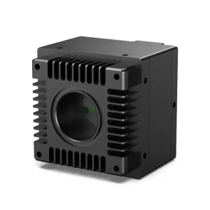
- Lens Mount and Mechanical Design: For optics, the cameras use a standard C-Mount lens interface, making them compatible with a wide range of machine vision lenses, including those corrected for NIR/SWIR wavelengths. The housing is a compact metal enclosure, roughly 64 mm × 64 mm × 56.5 mm in size and about 300 g in weight. Importantly, the body features mounting threads on five sides (all faces except the front lens opening), which gives flexibility in mounting orientation on industrial equipment or optical setups. This five-sided mounting design allows engineers to secure the camera from the top, bottom, or either side, which is very useful in tight spaces or when aligning multiple cameras. The enclosure is rated IP40 (protected from small objects >1 mm but not sealed against water) and the camera is specified for operating temperatures from -10 °C to 55 °C (non-condensing humidity 20–95%). These specs indicate robust operation in typical indoor lab or factory environments.
Applications in Industry and Research
The ability to image across both visible and SWIR bands makes these cameras versatile for many inspection, detection, and sensing applications. Some example use cases include:
- Semiconductor Inspection: In microelectronics manufacturing, SWIR imaging can see through silicon wafers and reveal subsurface features or defects that visible light cannot show. For instance, alignment marks buried under silicon, or cracks in silicon substrates, become visible in SWIR. The GD9L0’s dual-band camera can simultaneously capture the top-layer visible appearance of a wafer and SWIR details like circuit patterns on the backside or voids in bonded silicon stacks. This improves semiconductor testing and quality control.
- Solar Cell and Silicon Material Inspection: Short-wave IR is highly effective for examining silicon photovoltaic cells and wafers. Crystalline silicon is relatively transparent at wavelengths above ~1100 nm, so SWIR imaging can detect micro-cracks, inclusions, or soldering defects in solar cells that are invisible under visible light. The camera’s 0.4–1.7 μm range covers both the standard visual inspection of solar cell surfaces and SWIR analysis of silicon bulk quality and polycrystalline structure. This dual inspection helps in solar panel production (identifying defective cells) and in sorting silicon materials by purity or crystal type.
- Glass and Polymer Inspection: Many glass and plastic materials have different absorption/reflection characteristics in SWIR compared to visible light. For example, certain coatings, residues or internal stress patterns in glass cover plates (such as smartphone touch screens or optical components) are revealed under SWIR illumination. The GD9L0 camera can be used to inspect glass or polymer layers for contaminants, measure film thickness uniformity, or see through an optically opaque layer (to visible) that becomes translucent in SWIR. This is useful in quality control for display glass, coated optics, or multi-layer plastic films. The camera’s high dynamic range also helps to image glass, which can have both very bright reflections and dark absorption regions simultaneously.
- Automated Recycling and Sorting:Garbage classification systems benefit from the SWIR band because different materials (plastics, paper, organic matter, textiles, etc.) have distinct spectral signatures in the NIR/SWIR range. For instance, certain plastics that look similar in visible light can be differentiated by SWIR reflectance, enabling sorting machines to identify and separate them on a conveyor. A dual-band visible-SWIR camera can both “see” the object normally (for shape/size via visible light) and analyze material composition via SWIR. This improves accuracy in automated recycling facilities by identifying foreign objects or sorting waste streams by material type.
- Agriculture and Food – Fruit Defect Detection: Perhaps one of the most striking applications is detecting internal defects or bruises in fruits and produce. Bruises often do not show a visible mark on the surface initially, but the damaged tissue has higher water content and structural changes that strongly absorb **SWIR light (around 1000–1400 nm)**. Using the GD9L0 camera, a fruit can be imaged in dual bands to find “invisible” bruises: the visible-light image shows the fruit’s surface as normal, while the SWIR image will reveal dark spots where bruising or rot is present. This allows automated sorting systems to remove fruits with internal damage before they are visible to the human eye. It’s a powerful technique for quality grading of apples, pears, citrus, etc., improving consumer satisfaction and reducing waste.

6. Laser Spot Tracking and Active Imaging: Many industrial and scientific lasers emit in the NIR/SWIR range (for example, 1064 nm YAG lasers, 1550 nm telecom lasers, or certain IR fluorescence markers). The GD9L0 cameras can see laser beams or spots at these wavelengths for applications like laser spot tracking, beam profiling, or active illumination night-vision. For instance, a 1550 nm laser designator dot on a target is invisible to a normal camera but stands out clearly on an InGaAs sensor. Similarly in scientific imaging, some fluorescence or luminescence processes (such as NDVI imaging in plants, or SWIR quantum dots in biomedical imaging) emit light beyond 900 nm – which this camera can capture alongside the visible appearance of the subject. The ability to cover 0.4–1.7 μm in one device simplifies setups for multispectral imaging in research. Indeed, the manufacturer lists fluorescence imaging and laser spot tracking among key application areas for this dual-band camera.
Comparison with Other Visible+SWIR Cameras
Visible-to-SWIR imaging is an emerging capability, and a few other manufacturers have cameras in this category. The GD9L0-130CN-G2 / 33CN-G2 can be compared with similar dual-spectrum cameras in terms of resolution, speed, power, and spectral coverage:
- Hamamatsu C16741-40U: Hamamatsu Photonics recently released an InGaAs-based camera with the same 400–1700 nm sensitivity range and a 1280×1024, 5 µm pixel sensor. It similarly offers high resolution and broad spectrum imaging, presumably using a technology like a thin-film InGaAs that is responsive down to visible wavelengths. Hamamatsu’s model distinguishes itself with extremely low readout noise (achieved via a built-in TEC cooled sensor for thermal stability) and a USB 3.1 interface for data. The cooling improves its signal-to-noise for scientific use, and it supports 12-bit output over USB. However, the added Peltier cooler increases power consumption and device size. The GD9L0, by contrast, runs uncooled (<6 W) and uses GigE output; it may have slightly higher read noise, but it is more compact and network-integrable. In frame rate, the Hamamatsu C16741-40U is reported to run around 60 fps at full 1.3 MP, whereas the GD9L0-130CN-G2 is specified at 38 fps (likely a conservative number for GigE bandwidth). High-speed modes or ROI windowing could further boost the GD9L0’s rate if needed, but Hamamatsu’s USB3 throughput and low-noise design make it very strong for imaging throughput and sensitivity. Both cameras share the 5 µm pixel pitch which is a leap forward in SWIR imagery (older generation InGaAs sensors had larger ~15 µm pixels), enabling much higher resolutions in the same optical format.
- Xenics and “visSWIR” Cameras: Xenics (a specialist in IR imaging from Belgium) offers various SWIR cameras and has introduced dual-band capable models in recent years. For example, the Xenics Xeva 320 series is a 320×256 resolution SWIR camera that can be ordered in a “vSWIR” version – meaning an extended spectral response into the visible range. Those use InGaAs sensors with special modifications to detect some visible light (down to ~600 nm) while still reaching 1700 nm. Compared to the GD9L0 series, the older Xeva has much lower resolution but very high frame rates (up to 340 Hz) and requires CameraLink or USB interfaces. Xenics’ newer offerings include the Wildcat 1280 (also 1280×1024, 5 µm pixels) which likely uses the same generation of sensor as the GD9L0. The Wildcat/Goldeye cameras typically adhere to the GigE Vision or CameraLink standards and offer TEC cooling options. In general, Xenics and similar high-end SWIR cameras tend to provide cooling and higher frame rate at the cost of power. For instance, Allied Vision’s Goldeye G-130 VSWIR (which uses the same Sony 1.3 MP InGaAs sensor) can run at up to ~94 fps on GigE or 110 fps via CameraLink, but with an active cooler drawing ~12 W of power. The GD9L0-130CN-G2, without cooling, runs at 38 fps full-frame to stay within one GigE link’s bandwidth, prioritizing a simpler design and lower power draw. It’s a trade-off between raw speed and system simplicity: in many inspection scenarios 30–40 fps is sufficient, and the GD9L0 avoids the complexity of external frame grabbers or heavy cooling.
- Integration and Protocol Differences: One notable difference is that mainstream vis-SWIR cameras from companies like Allied Vision, Basler, or Hamamatsu often conform to machine vision standards (GigE Vision, GenICam or USB3 Vision) for ease of integration. The GD9L0 series uses a custom TCP/IP protocol with its own SDK – this provides flexibility (especially given the on-camera processing capability) but may require a dedicated integration effort into existing systems. On the other hand, the GD9L0’s embedded Linux and FPGA allow it to function more like a smart camera, potentially running user programs or interfacing directly with automation systems, which can reduce the need for a powerful host PC.
In summary, the GD9L0-130CN-G2 and GD9L0-33CN-G2 cameras represent a state-of-the-art solution for combined visible and SWIR imaging. They deliver SXGA or VGA-class resolution with a broad 0.4–1.7 µm response, enabled by modern InGaAs sensor technology. Compared to other vis+SWIR cameras on the market (e.g. Hamamatsu’s cooled scientific camera or Xenics/Allied’s high-speed offerings), the GD9L0 series distinguishes itself with its balanced design – offering high dynamic range and dual-band sensitivity in a compact, low-power GigE device with edge processing. This makes it particularly attractive for engineers and system integrators who need reliable, real-time dual-spectrum imaging in an industrial environment. By combining visible and SWIR capabilities, these cameras open up new possibilities in machine vision: from single-camera multispectral inspection systems to smarter sensors that can analyze materials, detect hidden features, and adapt imaging parameters on the fly – all within the camera itself.