


Single-Photon Avalanche Diodes (SPADs) are semiconductor p–n junctions biased beyond their breakdown voltage, operated in “Geiger” mode so that a single absorbed photon can trigger a self-sustaining avalanche of carriers. This avalanche produces a fast current spike (a digital “click”) that can be counted and time-tagged, enabling true single-photon sensitivity with picosecond timing resolution. Immediately after each avalanche the device must be quenched and reset to restore its bias; during this deadtime the pixel is insensitive to new photons. In practice, SPADs are built as either silicon (Si) devices (for UV–visible light) or InGaAs/InP heterostructures (for near-IR/telecom wavelengths). For example, an InGaAs SPAD pixel typically has an InGaAs absorption layer (to absorb 1000–1650 nm photons) bonded to an InP multiplication layer (to create the high field for impact ionization). An example SPAD-based photon-counting module is shown below – here the Excelitas SPCM (a silicon SPAD) used for visible/NIR detection. Such modules incorporate a SPAD and support electronics (quenching circuit, timing/discrimination) in a compact box.
In Geiger mode each photon creates a full avalanche, so the output is a fixed-amplitude pulse (no proportionality to photon energy), and the SPAD must be actively quenched and reset after each event. The high electric field in the multiplication layer ensures that even one photo-generated carrier will trigger a macroscopic current, yielding detection efficiency down to the single-photon level. Because the avalanche builds up very quickly, SPADs have intrinsically low timing jitter (often tens to hundreds of picoseconds), making them useful for time-resolved applications (the leading edge of the avalanche pulse marks the photon arrival time). However, the very high gain (and the use of wide-bandwidth electronics) also sets the noise floor: SPADs have a dark count rate (DCR) from thermally generated avalanches (often given in counts per second) that must be minimized for best sensitivity. Afterpulsing (spurious avalanches from trapped carriers) is another challenge in Geiger-mode operation, typically mitigated by adding delay (deadtime) before re-arming the SPAD.
Working Principles of SPADs
Operating a SPAD involves biasing it above breakdown and then carefully quenching each avalanche. In free-running mode the device is left continuously above breakdown; its internal quenching circuit (active or passive) must detect and stop each avalanche on a nanosecond timescale. Alternatively, in time-gated mode the bias to the SPAD is only applied for short windows synchronized to an expected photon arrival, which can suppress dark counts and afterpulses outside the gate. In either case, the SPAD produces a TTL/CMOS pulse for each detected photon, which can be routed to counters or a time-to-digital converter (TDC) for photon counting and timing.
Inside the SPAD pixel, the semiconductor structure typically includes a guard ring to prevent premature edge breakdown. For Si SPADs, back-illuminated and deep-trench isolation designs maximize the optical fill factor. For InGaAs/InP SPADs (1000–1650 nm), the epitaxial structure is tailored for IR sensitivity. Upon photon absorption, one carrier is swept by the electric field into the high-field region, where it gains energy and initiates impact ionization (creating more carriers and sustaining the avalanche). Once triggered, the avalanche is quenched by the front-end circuit (e.g. by momentarily lowering the bias below breakdown or using a series resistor) to reset the diode for the next photon. The deadtime and quench recovery set the maximum count rate per pixel. In modern designs this can be as fast as tens of MHz with advanced circuits. SPADs thus act as single-photon-sensitive “photon switches” – each photon yields one electronic pulse, after which the pixel must recover.
Evolution from Single-Pixel SPADs to SPAD Arrays
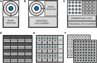
Originally SPADs were single-channel detectors, often used one at a time. Over time it became clear that having many SPADs in an array could massively speed up imaging and sensing tasks by capturing multiple spatial channels or parallel photon streams simultaneously. Early multi-pixel designs in the 2000s integrated a few SPADs with discrete electronics, and by the mid-2000s full SPAD arrays in CMOS began to appear. For instance, a 112×4 linear SPAD array was demonstrated in 2006, and a 128×2 array with on-chip timing was shown in 2007. These linear (1D) arrays arrange SPAD pixels in a row, with readout electronics placed at the edge. Linear arrays can achieve very high fill factor and low timing jitter (since each pixel can have its own quenching and TDC, unconstrained by pixel area).
In 2010, Princeton Lightwave announced a landmark 32×32 InGaAs SPAD focal-plane array with 100 µm pitch, each pixel having an active quench circuit and per-pixel timing electronics. This device, operating at 1.06–1.55 µm, used microlenses and a two-stage cooler to achieve low dark counts while delivering 200 kHz frame rates. In parallel, MIT Lincoln Lab and Hamamatsu developed similar 32×32 InGaAs/SPAD arrays for LiDAR and space applications. These early megapixel-scale SPAD imagers demonstrated that large 2D single-photon cameras for short-wave IR were feasible. More recently, research prototypes have scaled up even further – for example, a 64×64 InGaAs SPAD array was reported in 2022, pushing toward kilopixel SPAD cameras.
At the device level, integrating many pixels involves trade-offs. Each SPAD pixel requires quench and readout circuitry. In a monolithic CMOS SPAD array, these circuits share the same silicon as the photodiode, which can reduce the optical fill factor (the fraction of the pixel area that is photosensitive). Designers use techniques like backside illumination, microlens arrays (to focus light onto the active areas), and 3D-stacked architectures (separating the SPAD layer from the logic layer) to boost the effective fill factor. For instance, a stacked SPAD imager places the photodiodes on one layer and the CMOS timing/processing circuits on another, connected by copper (Cu-Cu) bonds【65†】. This approach, now used in commercial automotive LiDAR sensors, allows a very high pixel count (e.g. >100k pixels at 10 µm pitch) and a photon detection efficiency of ~22% at 940 nm.
Over the past decade, SPAD array technology has matured: PDE and noise have improved, timing resolution has sharpened, and pixel counts have grown. Modern InGaAs SPADs have seen dramatic efficiency gains – for example, >60% quantum efficiency at 1550 nm has been demonstrated in optimized APD structures (up from ~20% a few years earlier). Timing jitter of advanced InGaAs SPADs now reaches 50–100 ps FWHM, enabling sub-centimeter resolution in ToF systems. Dark count rates have also been greatly reduced by better material quality and cooling: researchers have achieved <1 kHz DCR (per pixel) at moderate PDE. Meanwhile, system innovations like GHz gating (self-differencing) and improved quench circuits have further suppressed afterpulsing, allowing higher count rates.
Challenges and Recent Innovations
Despite progress, SPAD arrays face challenges. InGaAs SPADs still have relatively high DCR and afterpulsing at room temperature, necessitating cooling (often to –30°C or colder). Scaling up arrays increases power and heat, complicating cooling. Crosstalk and uniformity across pixels must be addressed in layout. On the electronic side, integrating thousands of TDCs or counters on-chip (for each pixel) is nontrivial, requiring 3D-stacked circuits or row-wise time-encoding schemes.
Innovations continue to push the state of the art. Novel gating techniques (e.g. GHz sine-wave or self-differencing gating) allow InGaAs SPADs to operate at higher count rates with lower afterpulsing. Negative-feedback avalanche diodes (NFADs) incorporate a built-in resistor to passively quench avalanches, enabling simplified free-running operation. Backside illumination and Cu–Cu bonded 3D-stacked pixel chips (as used by Sony and others) greatly improve fill factor while keeping electronics underneath【65†】. Researchers are also exploring new materials (e.g. InGaAsP) and device architectures to boost quantum efficiency. Indeed, experimental InGaAs SPADs have reached >60% PDE at 1550 nm by optimizing the APD design, and jitter below 100 ps has become routine in lab devices. More complex gating and processing (e.g. on-chip histogramming or coincidence logic) are being integrated to enable real-time 3D imaging with SPAD arrays. The figure below illustrates a modern stacked SPAD sensor with photodiodes on top and CMOS timing circuits below, a configuration that yields high PDE and large arrays.
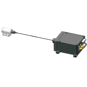
The LONTENOE OP500C InGaAs 4×4 SPAD Array
LONTENOE’s OP500C is a commercial 4×4 InGaAs/InP SPAD array component designed for single-photon detection in the 1000–1650 nm band. The device integrates sixteen InGaAs APD pixels (100 µm pitch, 0.4×0.4 mm total array area) with on-board fast quenching circuits, readout logic, and a thermoelectric cooler. Each pixel is read out independently, producing a TTL “pulse” per photon, and the deadtime per pixel is user-adjustable in firmware. The OP500C includes an integrated TEC module that cools the SPAD array to roughly –30 °C, dramatically suppressing dark counts.
According to the manufacturer’s specifications, the OP500C achieves about 10–15% photon detection efficiency (PDE) at 1550 nm under typical operating bias. The quoted PDE is specified at 10% minimum (15% typical) with a fixed deadtime of ~0.8 μs at –30 °C. Under these conditions each pixel’s dark count rate is on the order of 10^4 counts per second (≈10 kHz). The array’s output is a 16‑channel LVTTL connector (one output per pixel) plus a UART serial interface for parameter control. The whole assembly (with cooler and electronics) is compact – roughly 116×108×80 mm and about 300 g – making it easy to integrate into larger optical systems. In summary, the OP500C provides a turnkey 16‑pixel SPAD array in the NIR: each pixel with ~10–15% 1550 nm PDE, ~10 kHz dark counts, and TTL output pulses.
Comparative Analysis: LONTENOE SPAD Arrays vs. Other SPAD Detectors
The OP500C occupies a unique position among available SPAD detectors. Below we compare its key features with representative alternatives on the market:
Device | Channels | PDE @1550 nm | DCR | Timing Jitter | Cooling |
LONTENOE OP500C (InGaAs 4×4) | 16 (4×4) | 10–15% (typ.) | ~10 kcps per pixel (10% PDE) | ~200–300 ps (typ.) | Built-in TEC (∼–30 °C) |
ID Quantique ID230 (InGaAs) | 1 | up to 25% | ≲50–200 cps (at 25% PDE) | ~150 ps | Stirling (–90 °C) |
Excelitas SPCM-NIR (Si) | 1 | (not sensitive at 1550 nm; 73% @780 nm) | ~50 cps | ~300 ps (Si) | Peltier (~–10 °C) |
Princeton LW 32×32 (demo) | 1024 (32×32) | ~10–20% | ~1–10 kcps per pixel | (not published) | Dual-stage cryo |
Hamamatsu 32×32 (demo) | 1024 (32×32) | ~10–20% | ~1–10 kcps per pixel | (not published) | Dual-stage cryo |
- OP500C: The OP500C’s strength is its fully integrated 4×4 array in a compact package with onboard cooling and quench electronics. It offers 16 parallel single-photon channels – each with ~15% PDE at 1550 nm and ~10 kHz DCR – which is competitive for InGaAs SPADs of this pixel size. Its timing jitter (~200–300 ps) is higher than the best single-pixel SPD, but acceptable for many ToF applications. Because it is free-running with per-pixel quenching, it easily operates like four ID230s in one box. The built-in TEC (–30 °C) is particularly useful: it achieves low noise without bulky external coolers.
- ID Quantique ID230: The ID230 is a single-pixel InGaAs SPD module. It achieves up to ~25% PDE at 1550 nm and extremely low dark counts (tens of Hz) by using a Stirling cooler down to –90 °C. Its timing jitter is about 150 ps. Thus per pixel the ID230 outperforms OP500C’s pixels (25% vs 15% PDE; ≪1 kcps vs 10 kcps; ~150 ps vs ~300 ps). However, the ID230 provides only one channel. Building a 16-channel system would require 16 separate modules – bulky, expensive, and complex. In contrast, the OP500C supplies 16 channels in one unit. As LONTENOE notes, “ID Quantique remains the gold standard for single-pixel InGaAs SPAD performance, but the OP501C (and OP500C) carve out a more practical niche… offering 16 detectors in one integrated unit”.
- Excelitas SPCM-NIR: Excelitas’s SPCM-NIR is a silicon-based single-photon module designed for wavelengths up to about 900–1000 nm, not 1550 nm. It achieves ~73% PDE at ~780 nm, but silicon’s bandgap cuts off around 1.1 µm. Thus an SPCM-NIR has essentially zero efficiency at 1550 nm. Excelitas does not currently market a 1550 nm InGaAs SPD array. (Excelitas does sell InGaAs APD modules for linear detection, but not Geiger-mode arrays.)
- Princeton Lightwave (demo): Princeton Lightwave announced a 32×32 Geiger-mode InGaAs SPAD array (100 µm pitch) back in 2010. It featured on-chip quench and timing, microlenses, and cooling. This was mainly a research prototype for 3D imaging and not a commercial catalog product. According to reports, each pixel had on the order of 10–20% PDE and ~1–10 kHz DCR, similar to today’s SPAD arrays, but the module itself was large and power-hungry (two-stage cooler). Princeton has since moved on to larger-array projects, but no off-the-shelf InGaAs SPAD camera is available from them.
- Hamamatsu (demo): Hamamatsu Photonics (in collaboration with JAXA) developed a 32×32 InGaAs SPAD camera for eye-safe LiDAR. Again this was a specialized prototype (with microlenses and cooling) and not a standard product. Its pixels reportedly have ~10–20% PDE and ~1–10 kHz DCR, on par with OP500C’s pixel performance. However, Hamamatsu has not commercialized a multi-pixel InGaAs SPAD array for general sale.
In summary, the OP500C’s niche is providing a multi-pixel 1550 nm detector array in a compact, integrated module. While it doesn’t match the raw single-pixel sensitivity of a cryogenically-cooled ID230, it offers sixteen channels in one package with on-board cooling and control. This is advantageous for systems (LiDAR scanners, multi-channel QKD, prototype arrays) that need parallel detection. Its timing jitter (~300 ps) and PDE (15%) are modest by the strictest research standards, but are similar to other InGaAs arrays of this format. The integrated TEC and small form factor are distinctive: unlike a rack of single-SPD modules, the OP500C (and its module variant OP501C) operate from a single +12 V supply and weigh only a few hundred grams. In practice, one might trade a few dB of efficiency (15% vs 25%) for a 16× increase in parallel channels and a much simpler setup – exactly the cost–benefit that LONTENOE emphasizes for their product.
The OP500C’s unique features are thus its integrated multi-pixel format and cooling. Its onboard TEC (integrated Peltier cooler) brings the array to –30 °C without external chillers, which is uncommon for a compact InGaAs SPD array. Its per-pixel PDE (~15%) and jitter (~300 ps) are typical for monolithic InGaAs arrays of this size; where it differs is packaging. It weighs only ~0.3 kg and runs from a single 12 V supply, whereas achieving 16 channels with separate ID Quantique modules would be bulky and expensive. In short, the OP500C is not designed to beat single-pixel SPDs on raw performance, but to provide a practical 16-channel detector package for 1550 nm photon-counting.