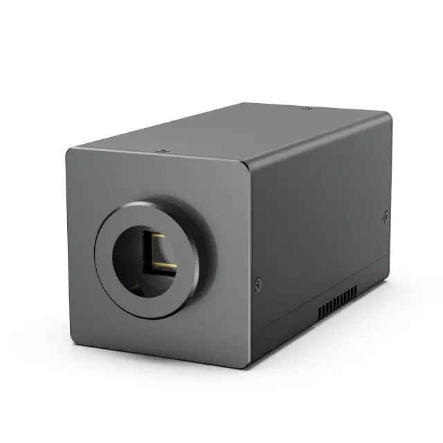
A InGaAs detection device is an instrument or component capable of accurately detecting and responding to minute changes in physical, chemical, or electrical signals. These devices are typically used in applications where detecting weak signals, such as light, sound, temperature, or motion, is critical, often used in scientific research, medical diagnostics, environmental monitoring, and advanced communication systems.
2.Typical application scenarios of Photoelectricity integrated devices:
quantum secure communication, quantum measurement, laser communication, site monitoring, early fire warning, forest fire prevention, driver vision enhancement, anti-counterfeiting and security inspection, photovoltaic chip inspection, silicon-based semiconductor material and process testing, laser optical detection, industrial temperature measurement, chemical detection, humidity monitoring.
3.Core Advantages of LONTEN:
Shortwave near-infrared range of 900nm-1700nm, extendable to 400nm-1700nm and 1000nm-2500nm; Features include large active area, high sensitivity, low noise, and high resolution, covering both cooled and uncooled types. High recognition capability, all-weather adaptability, equipped with low-light night vision and covert imaging characteristics, with a simple optical configuration. Possesses single-photon detection capability, fully autonomous and controllable from device to product, with internationally leading core technical specifications.
Data Download
Download catalogs, technical information, application notes, and product datasheets here.
InGaAs (Indium Gallium Arsenide) detectors have emerged as vital components in modern infrared sensing and imaging systems. These semiconductor devices excel at detecting light in the shortwave infrared (SWIR) spectrum. Their unique material properties, high sensitivity, and diverse applications have made them crucial in fields ranging from telecommunications to astronomy.
Fundamental Material Properties and Composition
InGaAs is an alloy of gallium arsenide (GaAs) and indium arsenide (InAs), belonging to the broader InGaAsP quaternary system of III-V compound semiconductors. The “III-V” designation refers to elements from Groups III and V of the periodic table, with gallium and indium from Group III and arsenic and phosphorus from Group V. This classification places InGaAs among a family of high-performance semiconductor materials with specialized optical and electronic properties.
The electrical and optical properties of InGaAs are largely determined by its energy bandgap, which can be tuned by adjusting the alloy composition. The energy bandgaps of the binary components in the InGaAsP system range from 0.33 eV (InAs) to 2.25 eV (GaP), with InP (1.29 eV) and GaAs (1.43 eV) falling in between.
Standard InGaAs typically has a composition of In₀.₅₃Ga₀.₄₇As, which is lattice-matched to InP and has a bandgap corresponding to a cutoff wavelength of approximately 1.7 μm. The lower bandgap compared to silicon makes InGaAs particularly well-suited for detecting near-infrared and shortwave infrared radiation that silicon-based detectors cannot efficiently capture. While silicon detectors typically have sufficient sensitivity only up to about 1100 nm (1.1 μm), InGaAs extends well beyond this limit, addressing an important gap in semiconductor detector technology.
InGaAs Detectors Performance Characteristics
Performance Characteristics
The performance of InGaAs detectors is characterized by several key parameters that determine their suitability for specific applications.
Spectral Response and Sensitivity
Standard InGaAs detectors typically offer spectral sensitivity from 0.9 to 1.7 μm, covering most of the SWIR band. This range corresponds to the bandgap of the InGaAs material with the standard composition. Extended variants can detect wavelengths up to 2.2 or 2.6 μm through adjustments in the material composition.
The photosensitivity of InGaAs detectors varies with wavelength, typically peaking in the near-infrared region between 1.3 and 1.6 μm. Responsivity-a measure of electrical output per optical input-typically ranges from 0.6 to 1.0 A/W at key wavelengths around 1550 nm.
Dark Current and Noise Considerations
Dark current-the current that flows through photodetectors even in the absence of light-represents one of the most significant limitations of InGaAs detectors. It is primarily caused by thermal excitation of electrons in the InGaAs material. The magnitude of dark current strongly depends on temperature, with a general rule of thumb that a temperature increase of 9 Kelvin approximately doubles the dark current. This temperature sensitivity necessitates cooling for many high-performance applications.
InGaAs detectors are affected by several noise sources that impact their signal-to-noise ratio:
Dark current noise: Generated by electron flow in the absence of light
Shot noise: Caused by the random arrival of photons
Thermal noise (Johnson noise): Generated by random thermal motion of electrons.
These noise sources collectively determine the detector’s noise-equivalent power (NEP), a measure of the minimum detectable power. Managing these noise sources is crucial for achieving optimal detector performance, particularly in low-light applications.
Structure and Operational Principles
Structure and Operational Principles
InGaAs photodetectors typically employ a PIN (Positive-Intrinsic-Negative) diode structure consisting of three primary layers:
P-type InGaAs layer: Doped with elements that provide extra holes (positive charge carriers)
Intrinsic (undoped) InGaAs layer: Serves as the absorption layer where the photoelectric effect takes place
N-type InGaAs layer: Doped with elements that provide extra electrons (negative charge carriers)
This three-layer configuration creates an electric field across the intrinsic region that efficiently separates photogenerated charge carriers. In modern focal plane arrays, the structure is more complex, typically including an InP substrate, an InGaAs absorption layer, and an ultrathin InP cap that is indium bump bonded to a readout integrated circuit (ROIC). This sophisticated architecture enables the creation of high-performance imaging systems.
The operational principle of InGaAs detectors is based on the photoelectric effect. When photons with sufficient energy strike the detector, they are absorbed in the intrinsic region, generating electron-hole pairs. Under an applied reverse bias, the electric field quickly separates these carriers, moving electrons toward the n-type layer and holes toward the p-type layer. This separation of charge carriers produces a photocurrent proportional to the intensity of the incident light, allowing the device to function as a light detector.
Types of InGaAs Detectors
Types
PIN Photodiodes
PIN photodiodes represent the most common type of InGaAs detector. These devices offer high sensitivity, relatively fast response times, and operation across the full InGaAs spectral range. The simple structure and reliable performance of PIN photodiodes make them the workhorses of InGaAs detection technology, widely used in telecommunications, spectroscopy, and various sensing applications.
Avalanche Photodiodes (APDs)
InGaAs Avalanche Photodiodes provide internal gain through the avalanche multiplication process. In these devices, a high electric field accelerates photogenerated carriers to energies sufficient to create additional electron-hole pairs through impact ionization. This internal gain mechanism makes APDs significantly more sensitive than standard PIN photodiodes, especially in low-light conditions.
Linear and Area Image Sensors
InGaAs technology has been extended to create both linear (one-dimensional) and area (two-dimensional) image sensors. Linear image sensors feature low dark current, low readout noise, and high scan rates, making them ideal for spectrophotometry, sorting machines, and process monitoring.
Area image sensors enable full two-dimensional imaging in the SWIR range, opening up applications in hyperspectral imaging, night vision, and machine vision. A typical InGaAs focal plane array consists of a two-dimensional photodiode array that detects SWIR incident light by collecting photon-generated charge. The readout integrated circuit (ROIC) converts this charge into voltage and transfers it to off-chip electronics to create an image. These imaging systems have transformed capabilities in numerous fields where seeing beyond the visible spectrum provides crucial information.
An InGaAs detector is a photodetector made of indium gallium arsenide, a semiconductor material sensitive to near-infrared (NIR) and short-wave infrared (SWIR) light.
InGaAs detectors are widely used in fiber-optic communications, spectroscopy, LiDAR, gas sensing, industrial inspection, SWIR imaging, and medical diagnostics.
Silicon photodiodes are limited to wavelengths up to ~1.1 µm, whereas InGaAs detectors extend sensitivity into the infrared, up to ~2.6 µm. InGaAs detectors have higher responsivity in the SWIR but are more expensive and have higher dark currents than silicon photodiodes.
At room temperature, dark current is usually in the nanoampere range for small detectors. Cooling significantly reduces dark current and improves performance.
Factors include detector size, spectral range, cooling type, and additional features like integrated amplifiers or array configurations. Larger, cooled, or extended-range detectors typically cost more.
InGaAs detectors have high responsivity and speed at the standard telecom wavelengths of 1.3 µm and 1.55 µm, making them ideal for high-speed data transmission.
Yes, especially InGaAs avalanche photodiodes (APDs), which are used for time-of-flight measurements and ranging applications in LiDAR systems operating at eye-safe wavelengths.
InGaAs detectors are commonly used in NIR absorption and Raman spectroscopy, as they can detect molecular vibrational and rotational transitions in the NIR/SWIR range.