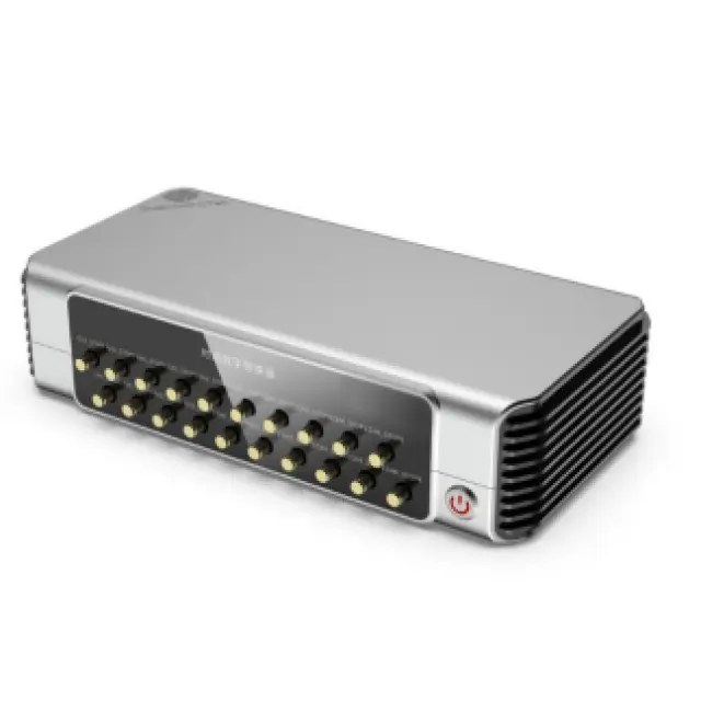


The QTDC-16CH-0A is a compact, high-precision measurement instrument featuring 16 acquisition channels and a time resolution of 10 ps. This time measurement device can record event time information in real time and supports the creation of histograms based on different bin values or statistical time settings. It also offers customizable features such as time coincidence detection and time-digit calculations. Utilizing 10G UDP Ethernet/USB3.0 interface protocols for raw data transmission, it enables secondary development and can be widely applied in scientific research fields such as laser after-pulse distribution measurement, quantum optics, and LiDAR.
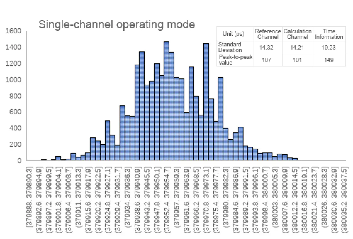
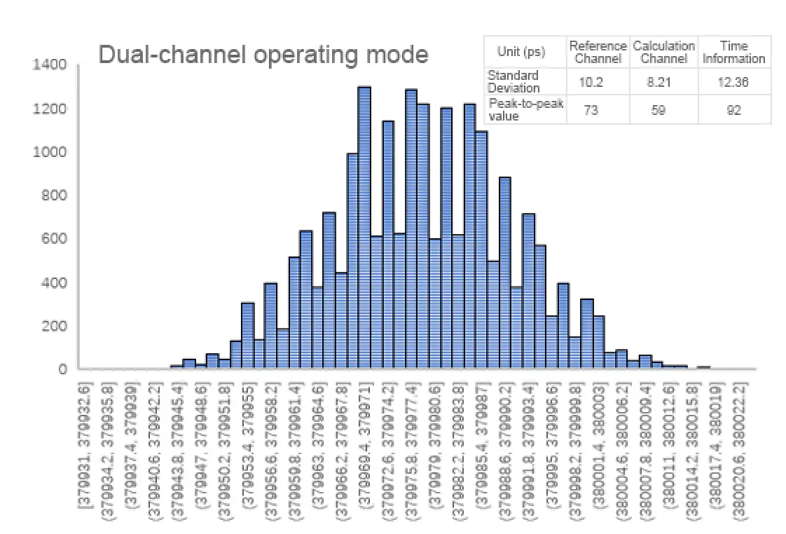
-16-channel raw time data acquisition
-10 ps time resolution
-Single-channel saturation count of 20 Mcps
-Jitter less than 20 ps
-Supports customized compliance counting function

522KB
| TECHNICAL PARAMETER | SPECIFICATION |
| Product Model | TDC-16CH-0A |
| Number of Channels | 4/8/16 |
| Time Measurement Resolution | <10 ps (related to working mode) |
| Standard Deviation (Std) | ≤ 20 ps (related to working mode) |
| Saturation Event Detection | 20 Mcps/channel |
| Dynamic Range | ≥ 1 ms |
| Interface Type & Input Impedance | SMA/50 Ω |
| Data Transmission Interface | 10G UDP/USB 3.0 |
| Configuration Interface | RS232 |
| Input Voltage Level | 3.3 V TTL |
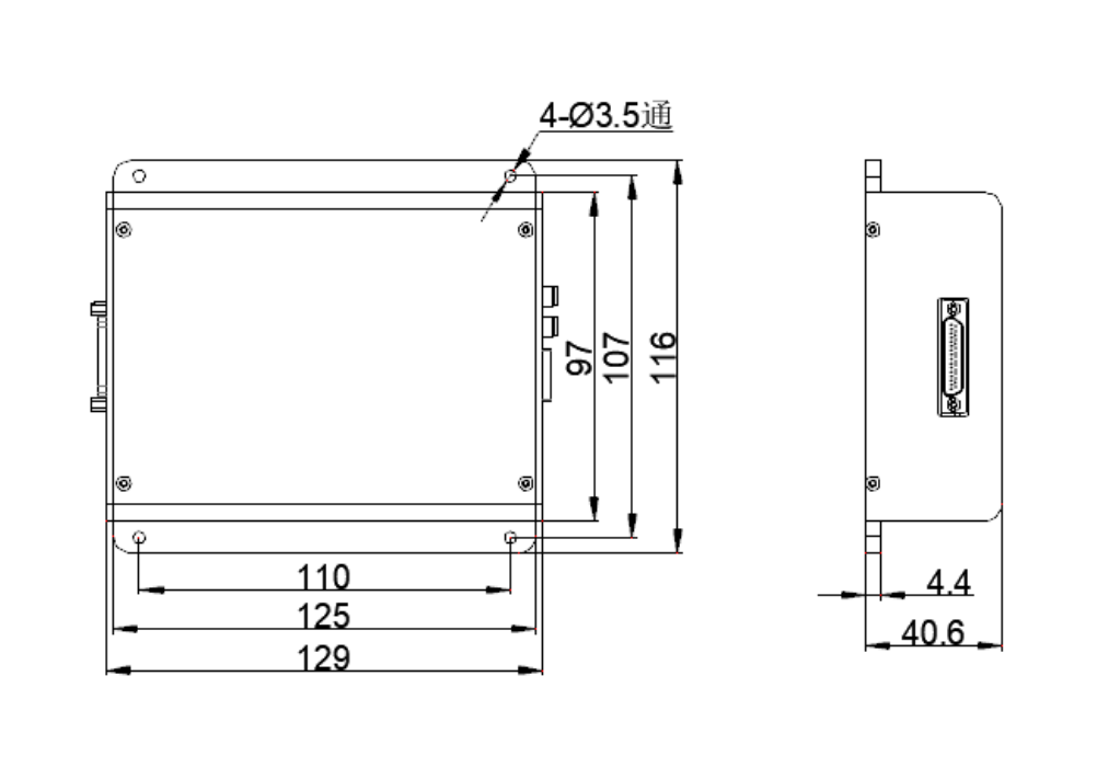
| Dimensions | ≤ 20 cm * 15 cm * 5 cm |
| Operating Temperature | -40°C to +125°C |
| Histogram Statistical Channels | 4 channels |
| Bin Setting | 2^m ps (m defaults to 3) |
| Frame Header | Length | Identifier | Sequence | CMD | Data | Checksum |
| Histogram 1 | A3A2_A1A0 | n | 0010_0000 | 0010_0001 | DATA0~n-1 | CHECKSUM |
| Histogram 2 | A3A2_A1A0 | n | 0010_0000 | 0010_0002 | DATA0~n-1 | CHECKSUM |
| Histogram 3 | A3A2_A1A0 | n | 0010_0000 | 0010_0003 | DATA0~n-1 | CHECKSUM |
| Histogram 4 | A3A2_A1A0 | n | 0010_0000 | 0010_0004 | DATA0~n-1 | CHECKSUM |
table 1-1
| Data Type | Frame Content |
| Odd Number of Data Points | {32’d0, Frame Header} {Length, Identifier} {Sequence, CMD} … {DATAn-1, Checksum} |
| Even Number of Data Points | {32’d0, Frame Header} {Length, Identifier} {Sequence, CMD} … {DATAn-2, DATAn-1} {Checksum, 32’d0} |
table 1-2
| Frame Content |
| {32’d0, Frame Header} {Length, Identifier} {Sequence, CMD} Data Checksum |
table 1-3
Format Example: 64’h0000_0000_A3A2_A1A0 (32’d2n, 32’h0020_0000) XXXX_XXXX_0000_0001 DATA0~n-1 CHECKSUM
| Field | Bit Range | Description |
| Data Header | [63:60] | Fixed Value: 8’hf5 |
| Channel Number | [59:56] | Values: 4’d0~4’d15 |
| Padding | [55:44] | Reserved: 12’d0 |
| TDC Data | [43:0] | 44-bit time data |
table 1-4
-Quantum optics and quantum communication
-Distance measurement and time measurement-related fields
-Lidar (Light Detection and Ranging), single-photon imaging
-Fluorescence lifetime and fluorescence spectroscopy
-Laser post-pulse detection, time-correlated counting
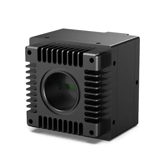
Visible Light⁺ Near-Infrared Camera
This camera is suitable for the spectral range of 400-1700nm, covering the visible light to shortwave
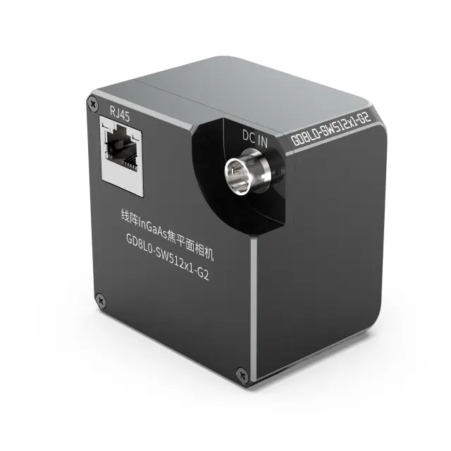
InGaAs Linear Focal Plane Camera
The industrial grade linear array shortwave infrared camera is designed for the spectral ange of 900-1700nm
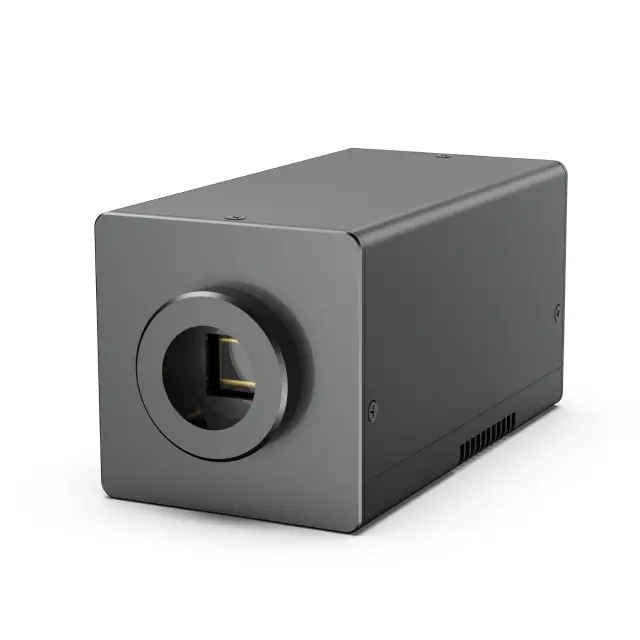
InGaAs Face Array Focal Plane Camera
This product uses domestically produced high sensitivity InGaAs array detectors, with array sizes of 320×256
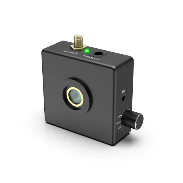
InGaAs Avalanche Photon Detector
This product is a compact near-infrared avalanche photodetector with a core circuit made of domestically

Time-to-Digital Converter
The QTDC-16CH-0A is a compact, high-precision measurement instrument featuring 16 acquisition
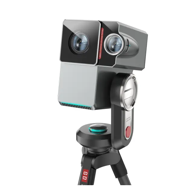
Single Photon Ranging System
This product adopts a fiber optic coaxial optical path design and an integrated system design,which has good stability
Time-to-Digital Converters (TDCs) are essential components in modern electronic systems that quantize time intervals into digital representations with high precision. These sophisticated devices bridge the analog and digital worlds by converting timing information into digital data that can be processed by computers and digital systems. This report provides a comprehensive overview of TDC technology, examining their fundamental principles, varied architectures, performance characteristics, and diverse applications.
A Time-to-Digital Converter (TDC) is a device that recognizes events and provides a digital representation of when they occurred. In essence, TDCs function like high-precision digital stopwatches, measuring the time interval between two signal events—typically referred to as “start” and “stop” pulses. They convert these time measurements into digital values that can be processed by digital systems.
The basic working principle of a TDC involves quantizing time intervals, often with the help of a counter that counts cycles of a reference clock fitting into the respective measurement interval between start and stop pulses. However, using only a counter limits resolution to the clock period, so various techniques are employed to achieve higher resolution.
TDCs can achieve remarkable precision, with resolutions ranging from nanoseconds down to just a few picoseconds. This makes them suitable for applications requiring extremely precise timing measurements. The measurement range can vary widely based on the TDC architecture, from nanoseconds to milliseconds.
For instance, the TDC7200 device from Texas Instruments provides a resolution of 55 ps with a standard deviation of 35 ps, and can operate in different modes supporting measurement ranges from 12 ns to 8 ms. Some advanced TDCs can achieve even higher precision, with resolutions down to 5 ps.
The simplest form of a TDC is based on counting the cycles of a reference clock that fit into the measurement interval. While straightforward to implement, this approach has limited resolution determined by the clock frequency.
In a counter-based TDC, the measurement interval defined by the start and stop signals is asynchronous to the reference clock signal. This causes measurement errors at the beginning and end of the time interval, limiting the accuracy. To address this limitation, various interpolation techniques are used to subdivide the reference clock cycle and improve resolution.
Delay line-based TDCs are more sophisticated and can achieve higher resolution than simple counter-based designs. In this architecture, the reference clock or start signal is delayed along a chain of delay elements. When the stop signal arrives, the delayed versions of the start signal are sampled in parallel, resulting in a thermometer code that represents the time interval.
The resolution of a delay line TDC depends on the delay of the individual elements in the chain. In Field Programmable Gate Arrays (FPGAs), the propagation delay of logic can be utilized to quantize time intervals using what’s called a Tapped Delay-Line (TDL). This approach allows for resolution in the nanosecond range even with clock frequencies of just a few hundred MHz.
To achieve even higher resolution, Vernier delay line techniques are employed. A Vernier TDC uses two delay lines with slightly different delay elements. The resolution is determined by the difference between the delays in the two lines, rather than the absolute delay value, enabling sub-gate delay resolution.
In a Vernier TDC, the start signal propagates through one delay line while the stop signal propagates through a second delay line with a shorter unit delay. The resolution is given by the delay difference between the two lines. This technique allows for extremely high resolution, with some implementations achieving resolution down to 5 ps.
Time amplification is another approach to improve TDC resolution. This technique stretches or amplifies the initial time interval before quantization, making it easier to measure with higher precision.
For example, a dual-slope TDC stretches the initial time interval by a large factor, allowing for easier quantization using a simple digital counter. Time amplifiers (TAs) can be key building blocks in two-step TDCs, with high-resolution TAs enabling picosecond-level precision.
TDCs can be implemented in various hardware platforms, including FPGAs and Application-Specific Integrated Circuits (ASICs). FPGA implementations offer advantages in terms of fast prototyping at low non-recurring engineering costs, while ASICs provide better performance but with higher development costs.
FPGA-based TDCs typically utilize the carry chain structure available in these devices, which allows for fine-grained delay control. Various techniques have been developed to improve the performance of FPGA-based TDCs, such as multi-chain designs and bin-width tuning methods.
ASIC implementations, on the other hand, can achieve higher resolution and better power efficiency. For instance, a CMOS TDC utilizing a Vernier delay line can achieve 30-ps resolution with accuracy exceeding ±1 LSB.
Resolution refers to the smallest time interval that a TDC can measure, typically expressed in picoseconds. It is a fundamental performance metric for TDCs, with modern designs achieving resolutions ranging from tens of picoseconds down to just a few picoseconds.
Precision, often measured by the standard deviation of repeated measurements, indicates the repeatability of the TDC measurements. High precision is critical for applications requiring consistent and reliable timing measurements.
Linearity is a critical performance characteristic of TDCs, typically measured using Differential Non-Linearity (DNL) and Integral Non-Linearity (INL). DNL refers to the deviation of the actual bin width from the ideal bin width, while INL represents the accumulated error across multiple bins.
Non-linearity in TDCs can arise from various sources, including process variations, temperature effects, and inherent asymmetries in the delay elements. Calibration techniques are often employed to compensate for these non-linearities and improve overall performance.
Power consumption is an important consideration, especially for battery-powered applications. Various techniques have been developed to reduce power consumption in TDCs, such as turning off oscillators when conversion is completed.
For instance, a gateable Vernier ring oscillator TDC can achieve ultra-low power consumption by employing a single-transition end-of-conversion detection circuit that turns off the ring oscillators whenever conversion is completed. This approach has achieved an average power consumption of just 1.2 mW with a resolution of 7.3 ps.
Calibration is essential for achieving high accuracy in TDCs, as it compensates for variations in delay elements due to process, voltage, and temperature fluctuations. Various calibration techniques have been developed, including on-the-fly calibration that continuously compensates for non-linearity without additional dead time.
For example, the TDC7200 from Texas Instruments uses a two-point calibration method to determine the actual least significant bit (LSB) value in real-time, ensuring accurate time-of-flight measurements across different environmental conditions.
TDCs are widely used in scientific research, particularly in high-energy physics experiments where precise timing of particle detection events is crucial. They can timestamp events with picosecond precision, enabling accurate measurements of particle properties and behaviors.
TDCs find extensive applications in distance measurement systems, such as laser range finders, LiDAR systems for drones, and ultrasonic flow meters. In these applications, TDCs measure the time-of-flight of signals (light, sound, or ultrasonic waves) to determine distance or flow rate.
For example, the TDC7200 is specifically designed for ultrasonic sensing measurements in water flow meters, gas flow meters, and heat flow meters. It can be paired with an ultrasonic analog front-end to form a complete ultrasonic sensing solution.
In all-digital phase-locked loops (ADPLLs), TDCs measure the phase shift between signals and provide feedback to adjust the digital controlled oscillator (DCO). This application is crucial in modern communication systems and digital clock generation circuits.
TDCs are essential components in medical imaging systems, particularly in time-of-flight applications such as positron emission tomography (PET) scanners. They enable precise timing measurements required for reconstructing high-quality medical images.
For instance, digital silicon photomultipliers incorporating TDCs can implement time-correlated single photon counting at rates far beyond conventional limits, enabling fast time-resolved scanning or ultrafast low-light event capture.
Time-to-Digital Converters represent a critical technology at the intersection of analog and digital electronics, providing the essential function of converting precise timing information into digital data. With continued advances in semiconductor technology and innovative architectures, TDCs are achieving ever-higher resolution, precision, and efficiency.
The versatility of TDCs makes them invaluable across diverse applications, from scientific research and medical imaging to consumer electronics and industrial measurements. As digital systems continue to evolve, the importance of accurate and efficient time-domain signal processing will only increase, further cementing the role of TDCs as fundamental building blocks in modern electronic systems.
Future developments in TDC technology will likely focus on further improving resolution and precision while reducing power consumption and size, enabling new applications and enhancing performance in existing ones. The ongoing convergence of time-domain and digital signal processing represents a promising direction for addressing the challenges of next-generation electronic systems.
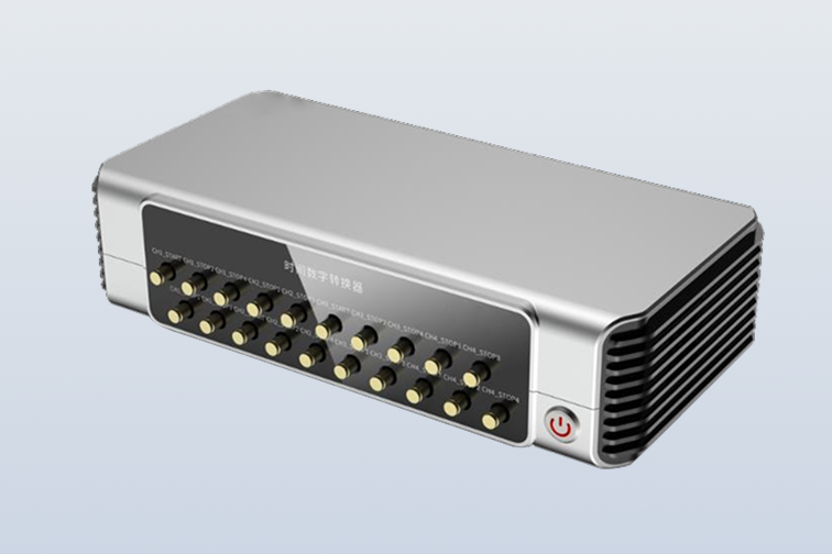
A Time-to-Digital Converter (TDC) is a device that measures the time interval between two events—typically a “start” and “stop” signal—and converts this interval into a digital output. It functions as a high-precision stopwatch, with resolutions ranging from nanoseconds to picoseconds, depending on the architecture. TDCs are critical in applications requiring precise timing, such as particle physics experiments, LiDAR systems, and ultrasonic flow meters.
TDCs use advanced architectures like Vernier delay lines or time amplification techniques to subdivide clock cycles into finer intervals. For example, Vernier TDCs employ two delay lines with slightly different propagation delays, enabling resolution determined by the difference between delays (e.g., 5 ps). Stochastic TDCs leverage process variations in CMOS technology and statistical methods to achieve sub-picosecond resolution.
Common architectures include:
Delay Line TDCs: Use a chain of delay elements to quantize time intervals. The resolution depends on the delay per element, often achieving nanosecond precision in FPGAs.
Vernier Delay Line TDCs: Employ two delay lines with mismatched delays for sub-gate resolution.
Ring Oscillator TDCs: Rely on oscillating loops of inverters to measure intervals, suitable for low-power applications.
Stochastic TDCs: Utilize statistical methods and self-calibration to compensate for process variations, achieving sub-picosecond resolution.
FPGA-based TDCs (e.g., Xilinx Kintex-7) use programmable logic blocks and delay chains, offering rapid prototyping and resolutions down to 3.9 ps. ASIC implementations, such as the TDC7200, provide higher precision (55 ps resolution) and lower power consumption (0.5 µA at 2 SPS) but require custom fabrication.
Resolution: Smallest measurable time interval.
Linearity: Differential (DNL) and integral (INL) non-linearity, often improved via calibration.
Power Consumption: Ranges from 1.2 mW in Vernier ring oscillators to 6.16 mW in LiDAR systems.
Measurement Range: From nanoseconds to milliseconds.
TDCs use advanced architectures like Vernier delay lines or time amplification techniques to subdivide clock cycles into finer intervals. Stochastic TDCs leverage process variations in CMOS technology and statistical methods to achieve sub-picosecond resolution.
Yes. Some devices support supply voltages from 2–3.6 V and temperatures from -40°C to 85°C, making them suitable for industrial and automotive applications.
Miniaturization and integration with sensors (e.g., in 130 nm CMOS processes) allow TDCs to occupy <0.03 mm², enabling portable flow meters and health monitors.