


Definition and Operating Principles of Photodiode Arrays
A photodiode array is an assembly of multiple photodiodes integrated into a single device or chip. Each photodiode is a p-n junction semiconductor that generates an electrical current when exposed to light (photons), via the photovoltaic effect. In an array, each photodiode element (often called a pixel) operates independently, converting incident photons into current or charge. The key operating principle is the same as for a single photodiode: absorbed photons create electron-hole pairs in the semiconductor, and under reverse bias these carriers are swept into the external circuit as photocurrent. By arranging many photodiodes in a grid or line and connecting them to appropriate readout circuitry, one can measure spatially resolved light intensity across the array.
Photodiode arrays can be configured in different geometries. Linear arrays are one-dimensional strips of photodiodes, while area arrays (two-dimensional) consist of pixels arranged in rows and columns (similar to a camera sensor). Each pixel in the array has its own electrical output (or is multiplexed into shared outputs) so that light intensity at each pixel can be measured. To prevent signal loss and interference, array devices often integrate readout electronics or multiplexers to quickly scan and output the signals from potentially hundreds or thousands of pixels in parallel or sequentially. Photodiode arrays may operate in photovoltaic mode (zero bias) or photoconductive mode (reverse bias for faster response at the cost of higher dark current). In either case, the array’s performance depends on the efficiency of converting photons to electrons (quantum efficiency), the noise characteristics of each photodiode, and the quality of the readout circuit.
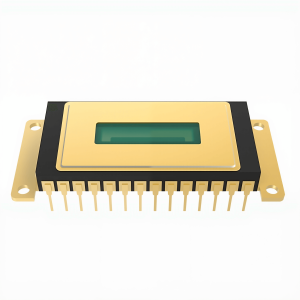
For proper operation, photodiode arrays often require careful design of the readout interface. In many imaging arrays, a CMOS or CCD readout integrated circuit is bump-bonded or monolithically integrated with the photodiodes. This captures the charge or current from each photodiode and converts it into a voltage or digital signal. For example, in a hybrid InGaAs infrared focal plane array, a CMOS readout chip is flip-bonded to an InGaAs photodiode array chip. This way, each pixel’s photocurrent is amplified and read out with minimal noise, enabling the array to achieve high sensitivity and fast readout speeds.
Types of Photodiode Arrays
Photodiode arrays come in several types, distinguished by their geometry and the technology used:
Linear Photodiode Arrays (1D Arrays)
A linear photodiode array is a one-dimensional strip of photodiodes, typically arranged in a straight line with equal spacing. These arrays might contain anywhere from a few elements to thousands, depending on the application. Linear arrays are widely used in spectrometers and line-scan cameras. In a spectrometer, for example, light dispersed by a prism or grating is projected onto a linear photodiode array so that each pixel measures the intensity at a different wavelength. This allows rapid acquisition of an entire spectrum simultaneously. In a line-scan camera or imaging system, a linear array can capture one row of an image at a time (useful for scanning moving objects or conveyor belts).
Linear arrays often feature elongated pixel shapes to increase light collection area. For instance, a linear InGaAs array might have pixels that are 25 µm wide by 500 µm tall. The long pixel height helps capture more photons from a spectrometer slit or line image without gaps between pixels. An example is Lontenoe’s InGaAs linear array with 1024 pixels of size 25×500 µm, in a hermetically sealed metal-ceramic package. Hamamatsu Photonics similarly produces InGaAs linear arrays (e.g. 512 or 1024 elements) for NIR spectrophotometry. Such devices were even employed in space; a Hamamatsu InGaAs linear sensor was used in JAXA’s Hayabusa asteroid explorer for multi-channel spectroscopy.
Key considerations for linear arrays include pixel count, pitch (spacing), and readout speed. Because only one line of pixels is present, these arrays are read out sequentially (or in parallel chunks) very quickly. They can achieve high line rates (thousands of lines per second), enabling high-speed scanning. Many linear arrays offer low-noise performance and even cooling options if targeting low-light applications. Some specialized linear arrays exist for X-ray or other radiation (often with scintillators), but in the context of photodiodes we mainly refer to optical/NIR detectors. Linear photodiode arrays have the advantage of simpler readout electronics compared to 2D arrays and are often easier to calibrate for uniformity in spectroscopy applications.
Two-Dimensional Photodiode Arrays (Area Image Sensors)
Two-dimensional photodiode arrays consist of pixels arranged in a grid covering an area, and they function as image sensors or focal plane detectors. The most common example is the sensor in a digital camera, which is effectively a silicon photodiode array with millions of pixels (often implemented as CMOS or CCD technology). Each pixel records the intensity of light at a specific location in the image. In advanced scientific and industrial contexts, 2D photodiode arrays are made from various materials to detect different wavelength bands (e.g. silicon for visible, InGaAs for short-wave infrared, HgCdTe for mid-wave infrared, etc.). These arrays are central to focal plane arrays (FPAs) used in thermal imaging, night vision, astronomy, and microscopy.
A typical photodiode imaging array integrates each photodiode with an active readout circuit in each pixel (as in CMOS Active Pixel Sensors) or with multiplexing circuits that read each pixel sequentially (as in CCDs or hybrid FPAs). For example, an InGaAs area sensor for SWIR (0.9–1.7 µm) might have 320×256 pixels at 30 µm pitch, bonded to a CMOS readout chip. Lontenoe’s 320×256 InGaAs FPA is built exactly this way: InGaAs photodiodes on an InP substrate are inverted and interconnected with a CMOS readout IC, creating a hybrid FPA with low noise, high uniformity, and large dynamic range. The device can operate with or without cooling, but integrating a thermoelectric cooler (TEC) in the package improves low-light performance and stability. Such cooling reduces the dark current and noise, which is especially important for infrared photodiodes.
Modern 2D photodiode arrays often have advanced features like adjustable integration times, multiple output channels for faster readout, windowed readout modes, and high frame rates. For instance, the Lontenoe 320×256 InGaAs sensor supports 1, 2, or 4 parallel output ports and can reach up to 300 frames per second with 4-port readout. Similarly, Hamamatsu’s InGaAs area sensors include models with 320×256 resolution at 20 µm pitch that achieve up to ~500 fps using four outputs. These area arrays find use in applications like hyperspectral imaging, industrial sorting, machine vision, and surveillance. The broad applicability comes from their ability to form real-time images or image-like data.
It’s worth noting that many visible-light imaging sensors (CCD or CMOS cameras) are effectively photodiode arrays too (silicon photodiodes for each pixel, with built-in transistor readout). However, the term “photodiode array” is often used in contexts where the array is primarily a sensor without complex on-chip image processing – for example, photodiode arrays used in spectroscopy or simple cameras, as opposed to full consumer camera sensors with color filters and image processing. Nonetheless, the operating principles are similar.
Avalanche Photodiode Arrays and SPAD Arrays
Avalanche photodiodes (APDs) are a special class of photodiodes that operate at high reverse bias voltage, causing carriers from absorbed photons to undergo impact ionization. This produces an avalanche multiplication of the charge, providing internal gain. APDs can be significantly more sensitive to weak light than regular photodiodes because each photon can trigger a cascade resulting in a larger current pulse. However, APDs introduce excess noise due to statistical variations in the multiplication process. When multiple APD pixels are integrated in one device, we get an APD array, which is useful for applications requiring multiple highly sensitive detector channels (for example, multi-pixel rangefinders, LiDAR receivers, or PET scanners).
Avalanche photodiode arrays are commonly implemented in silicon for detection of visible to near-infrared (up to ~1000 nm) and in InGaAs or other compound semiconductors for longer NIR (e.g. 1550 nm) detection. Silicon APD arrays have seen extensive use in LiDAR (laser ranging) systems that use 905 nm laser pulses. For instance, First Sensor (now part of TE Connectivity) produces monolithic silicon APD arrays specifically for LiDAR, including linear arrays (e.g. 8 or 16 pixels in a row) and matrix arrays up to 64 pixels. These APD arrays are optimized for fast response around 900 nm with high quantum efficiency (>80%) in that band. They feature low capacitance and fast rise times to accurately detect short laser pulses. An example is First Sensor’s 16-pixel linear APD array, which comes in a compact SOJ package and offers multiple elements on a single chip for parallel rangefinding. Such arrays often include a built-in thermistor for temperature monitoring (to stabilize gain, since APD gain is temperature-dependent) and are sometimes provided with pre-amplifier modules for convenience.
Another approach to avalanche photodiode arrays is to operate each pixel in Geiger mode, where the APD is biased above the breakdown voltage so that a single photon can trigger a self-sustaining avalanche. Each pixel in this mode is essentially a SPAD – Single-Photon Avalanche Diode. SPAD arrays are digital in nature: each pixel output is a binary event (photon detected or not within a given time window), and after each detection the pixel must be “quenched” (the avalanche stopped via a quench resistor or active circuit) and reset. SPAD arrays allow for single-photon sensitivity across multiple pixels and are increasingly popular for applications like time-of-flight 3D cameras, fluorescence lifetime imaging, and quantum communication.
SPAD arrays have been developed in silicon (for visible light) by several manufacturers. Hamamatsu, for example, offers MPPC (Multi-Pixel Photon Counter) devices, which are essentially arrays of many tiny SPAD microcells operating in unison (the outputs summed to produce an analog signal proportional to the photon count). These achieve high photon detection efficiency with low crosstalk and low afterpulsing. For instance, Hamamatsu’s S13360 series MPPC arrays have multiple Si SPAD pixels and feature low dark count rates and crosstalk, making them suitable for precision measurements down to the single-photon level. Some MPPC/SiPM arrays are arranged in multi-channel formats (e.g. 4×4 or 8×8 arrays of larger pixels) for use in systems like PET scanners or lidar sensors. The Hamamatsu S16786 is a near-IR sensitive SiPM optimized for automotive LiDAR, featuring smaller SPAD microcells to improve dynamic range while still maintaining high photon detection efficiency in the 905 nm range.
In the infrared (telecom wavelengths ~1310–1550 nm), making SPAD arrays is more challenging due to higher dark noise in materials like InGaAs. Nevertheless, Lontenoe and a few other specialized companies have developed small InGaAs SPAD arrays. Lontenoe offers a 4×4 InGaAs SPAD array assembly that combines a 16-pixel InGaAs SPAD chip with a CMOS quenching/readout circuit chip. Each pixel can detect single photons in the 0.95–1.65 µm band, and the design uses both active and passive quenching to reset the diodes after each photon event. The 4×4 SPAD array has a pixel pitch of 100 µm and achieves photon detection efficiency (PDE) of roughly 10–25% in its spectral range. To improve performance, the SPAD array module includes cooling (a “refrigeration module”) and support electronics. This allows the array to operate with lower dark counts, which is crucial for single-photon counting in the IR. Such technology is cutting-edge – whereas silicon SPAD arrays are more common, InGaAs SPAD arrays address applications like laser ranging at eye-safe 1550 nm, quantum key distribution, and IR fluorescence detection where single-photon sensitivity is needed.
In summary, avalanche photodiode arrays (including SPAD arrays) extend the functionality of photodiodes into extremely low-light regimes and fast timing applications. They do so at the cost of added complexity: each pixel might need a high-voltage bias and either a quench resistor (for passive quenching) or a fast active circuit to stop avalanches. The array structure must also minimize crosstalk (a triggered avalanche in one pixel inducing spurious triggers in neighbors via electrical or optical coupling). Despite these challenges, APD and SPAD arrays are increasingly important in remote sensing and imaging. For example, in LiDAR, a linear APD array with 64 pixels can act as a “row” of receivers capturing a reflected laser stripe to form a 3D point cloud of the environment. Each pixel in the 1×64 array corresponds to a small angle in the field of view, collectively yielding high-resolution distance information. Excelitas Technologies recently introduced such a 1×64 Si APD array for next-generation automotive LiDAR, noting that the high pixel count enables using smaller optics and achieving longer detection range beyond 200 m for vehicles. The array is packaged in a compact surface-mount module and can be customized in pixel size and count to suit different optical designs.
Material Considerations: Silicon vs. InGaAs Photodiode Arrays
The choice of semiconductor material in a photodiode array directly determines its spectral sensitivity, noise characteristics, and suitable applications. Silicon (Si) and Indium Gallium Arsenide (InGaAs) are two of the most common materials for photodiodes, each covering different parts of the spectrum:
- Silicon Photodiode Arrays: Silicon has a bandgap of 1.12 eV, which means silicon photodiodes are responsive to photons with wavelengths roughly from the UV (~190 nm) up to about 1100 nm (just into the near-infrared). Silicon photodiode arrays are widely used for visible light detection and have excellent performance in the 400–900 nm range with quantum efficiencies often above 80%. They can be fabricated at high volume using standard silicon processes, enabling large arrays with small pixel sizes (down to a few microns for CMOS imagers). Si devices generally exhibit low dark current at room temperature, especially for small pixels, which leads to low noise. For example, a silicon PIN photodiode might have dark current in the picoampere range. Cooling is usually not required for Si photodiode arrays in visible-light applications, except in extremely low-light or scientific scenarios. Silicon’s combination of maturity and performance makes it ideal for camera sensors, silicon APDs for 905 nm LiDAR, and dense arrays like silicon photomultipliers.
- InGaAs Photodiode Arrays: InGaAs is a compound semiconductor that can be tuned in composition to adjust its bandgap. The most common alloy (In₀.53Ga₀.47As lattice-matched to InP substrates) has a bandgap corresponding to a cutoff wavelength of ~1.7 µm. Standard InGaAs photodiodes thus cover approximately 0.9 µm to 1.7 µm spectral range, which includes the important telecommunication bands (1310 nm and 1550 nm) and the short-wavelength infrared (SWIR) imaging range. InGaAs arrays are the go-to solution for SWIR imaging and sensing. They typically achieve high quantum efficiency as well – often ≥70–80% in their band (for instance, Lontenoe’s 320×256 InGaAs FPA has QE ≥75% from 1.0 to 1.6 µm). Compared to silicon, InGaAs photodiodes generally have higher dark currents when uncooled, due to the smaller bandgap (0.75 eV for InGaAs vs 1.12 eV for Si). Therefore, cooling (with a TEC or liquid nitrogen for extreme cases) is frequently used to reduce thermal noise for sensitive applications.
InGaAs arrays are more expensive and lower density than silicon ones, primarily because they are often hybrid devices: the photodiodes are made on an InP wafer and then bump-bonded to a silicon CMOS readout. This hybrid approach is necessary since one cannot monolithically integrate a full CMOS circuit in InGaAs material. Despite this complexity, high-performance InGaAs FPAs are available from several manufacturers. They come in formats like 320×256 or 640×512 with pixel pitches typically 15–30 µm. Some InGaAs arrays also offer extended wavelength ranges: by adjusting the alloy or using InGaAsSb, the cutoff can be pushed to 2.2 µm or even 2.6 µm (at the expense of higher dark current). Conversely, some “visible extended” InGaAs has a thinner absorption layer to detect down around 600–800 nm, albeit with reduced efficiency at those wavelengths. Lontenoe’s FPA, for example, is offered in a variant that extends down to 0.4 µm – this likely indicates a specialized design allowing detection of some visible light (perhaps by having a dual-layer absorber or a very thin InGaAs layer so blue/green light can reach it). Hamamatsu also lists InGaAs photodiodes with response starting around 0.5 µm, which hints at a similar extended-range technology.
InGaAs photodiode arrays are indispensable for SWIR imaging (used in fiber optic inspection, semiconductor inspection, night vision, etc.) and for optical communication monitoring. For instance, arrays of InGaAs photodiodes are used in DWDM (Dense Wavelength Division Multiplexing) fiber optic systems to monitor multiple wavelength channels simultaneously; a 40-channel InGaAs PIN photodiode array with 250 µm channel pitch is designed for such DWDM monitoring, offering low crosstalk and precise alignment of elements.
In summary, Si vs InGaAs often comes down to spectral range and noise. Silicon is excellent for visible light and can be integrated at high density, with low noise at room temperature. InGaAs covers the IR beyond silicon’s limit, but typically requires cooling for low-noise performance and is limited to smaller array sizes due to cost and fabrication complexity. In many instruments, both types coexist: for example, a spectrometer might use a Si photodiode array for 400–900 nm and an InGaAs array for 900–1700 nm to cover a broad spectrum. Likewise, for LiDAR, silicon APD arrays serve 905 nm systems, while InGaAs APD or SPAD arrays are used for eye-safe 1550 nm laser systems.
Other materials beyond Si and InGaAs include HgCdTe (MCT) for mid-IR, InSb for 1–5 µm, and even Geiger-mode APDs in HgCdTe for long-wave IR single-photon detection. However, those are specialized and beyond the typical scope of “photodiode arrays” in general discussion, which usually centers on Si and InGaAs for UV/VIS/NIR/SWIR detection.
Common Applications of Photodiode Arrays
Photodiode arrays are employed across diverse industries and research fields. Below are some common applications:
- Spectroscopy: Photodiode arrays (especially linear arrays) are widely used in spectrometers and multi-channel optical analyzers. When dispersed light falls on a linear array, each photodiode measures a different wavelength, enabling simultaneous capture of an entire spectrum. This is the principle behind Photodiode Array Spectrophotometers (PDAs). They allow rapid spectral scans without moving parts, ideal for chemical analysis, environmental monitoring, and astronomy. For example, the HAYABUSA asteroid probe used a Hamamatsu InGaAs linear photodiode array to analyze surface spectra on the asteroid.
- Imaging and Machine Vision: Two-dimensional photodiode arrays form the sensors in cameras and imaging systems. Silicon CMOS and CCD sensor arrays are ubiquitous in consumer cameras, microscopes, and telescopes. In industrial machine vision, specialized arrays (including InGaAs FPAs) are used for imaging in spectral bands beyond human vision (e.g. SWIR imaging can distinguish materials, see through certain packaging, or image through smoke/fog). Hamamatsu notes that their InGaAs area sensors are used in hyperspectral imaging, industrial sorting, process inspection, etc.. SWIR cameras employing InGaAs arrays can inspect solar cells, textiles, and produce thermal images in certain ranges. Photodiode arrays are also found in optical mice and sensors, where a small array tracks movement relative to a surface.
- LiDAR and Rangefinding: As discussed, avalanche photodiode arrays are key to LiDAR (Light Detection and Ranging) systems. In automotive LiDAR, for instance, an array of APDs or SPADs detects returning laser pulses from multiple directions to map the environment. A linear APD array with many pixels can receive light from a broad swath when paired with a rotating mirror or a diffractive element. The Excelitas 1×64 Si APD array is explicitly designed for high-resolution LiDAR, improving object detection around vehicles. Each pixel in such arrays effectively corresponds to a “range channel.” SPAD arrays also enable flash LiDAR, where a 2D SPAD array (e.g. 32×32 or 64×64 in research prototypes) captures a depth image from a single laser flash, with time-of-flight measured per pixel. Beyond autonomous vehicles, LiDAR APD arrays are used in surveying, forestry (lidar mapping of terrain and vegetation), and even in some biometric sensors (like facial recognition 3D cameras on mobile devices, which use small SPAD arrays).
- Telecommunications and Fiber Optics: Photodiode arrays monitor optical signals in fiber optic networks. For example, in wavelength-division multiplexing, an array of photodiodes can be aligned under an array of diffracted beams or filters to monitor the power in many channels simultaneously. Arrays are also used in coherent receivers and other advanced optical communication systems to detect multiple polarization or phase components. In high-speed optical links, arrays of photodiodes may be paired with arrays of VCSEL lasers for parallel fiber links.
- Medical Imaging and Sensors: In medical imaging, arrays of photodiodes are used in devices like CT scanners and PET scanners (when coupled to scintillators). Specifically, silicon photomultipliers (SiPM arrays, which are arrays of SPADs) are increasingly used in PET detectors to capture the scintillation photons from gamma ray interactions. These arrays offer the advantage of compactness and robustness over traditional PMTs. Hamamatsu’s MPPC arrays, for example, are offered in tiling-friendly packages with minimal dead space for building larger imaging panels in PET scanners. Photodiode arrays also find use in pulse oximetry sensors (multi-wavelength photodiode arrays to detect oxygen saturation) and in some bioanalytical instruments (like microplate readers that use an array to scan multiple wells simultaneously).
- Scientific Research: Researchers use photodiode arrays in a variety of experiments. SPAD arrays are used in **fluorescence lifetime imaging microscopy (FLIM)**, where each SPAD pixel times photon arrivals to map molecular environments. Large-area photodiode arrays are used in particle detectors and nuclear physics (e.g. silicon strip detectors or pixel detectors in high-energy physics are essentially photodiode arrays detecting charged particles via ionization). Astronomers use photodiode array detectors for certain IR telescopes or spectrographs. The academic research sector often employs MPPC/SiPM arrays for physics experiments (they appear in experiments for scintillator-based detectors, LIDAR research, quantum optics, etc.).
- Environmental and Safety Monitoring: Arrays of photodiodes can be used in electronic nose (e-nose) or optical biosensor devices where multiple sensing elements detect various gases or biomolecules (with each photodiode reading out an optical sensor’s response). In radiation detection, linear diode arrays (LDAs) scan X-ray images in some older CT systems or in security scanners (each photodiode behind a scintillator stripe, scanning line by line).
In all these applications, photodiode arrays provide the advantage of capturing spatially resolved or multi-channel data in a single snapshot or a fast scan, which is often far more efficient than using single photodiodes moved mechanically or multiplexed slowly. The choice of array type and material will depend on the specific wavelengths, speed, and sensitivity requirements of the application.
Key Performance Metrics for Photodiode Arrays
When evaluating photodiode arrays, engineers and scientists consider several important performance metrics:
- Spectral Response and Quantum Efficiency (QE): This describes the range of wavelengths the array can detect and how efficiently it converts photons to electrical signal. It is often given as a spectral response curve or a range (e.g. “0.9–1.7 µm” for InGaAs, or 400–1100 nm for Si). Quantum efficiency is the fraction of incident photons that generate charge carriers; e.g. a QE of 80% means 80% of photons hitting the photodiode produce electron-hole pairs. High QE is desirable for sensitivity. In practice, QE can be wavelength-dependent; for instance, Lontenoe’s InGaAs array achieves ≥75% QE in the 1.0–1.6 µm band. Sometimes a photodiode’s responsivity is quoted instead – responsivity (in A/W) relates to QE but weighted by photon energy (it’s the output current per unit optical power). For example, a Si photodiode might have ~0.4 A/W at 500 nm and ~0.6 A/W at 800 nm; InGaAs might be ~1.0 A/W at 1300 nm. A higher responsivity or QE means more signal for a given light intensity.
- Pixel Count and Pixel Size: The number of pixels (elements) in the array and their size/pitch define the spatial resolution and active area. A higher pixel count (e.g. a 1024-element linear array vs a 128-element one) gives finer detail or spectral resolution, but often each pixel is smaller, which can limit the light collection area per pixel. Pixel size matters because it influences both sensitivity (larger pixels collect more light) and capacitance (larger junctions have higher capacitance, which can slow the response). There’s a trade-off between resolution and per-pixel sensitivity. As an example, Hamamatsu’s 320×256 SWIR sensor has 20 µm pixels, whereas Lontenoe’s of the same format has 30 µm pixels – the former prioritizes higher spatial resolution, while the latter might achieve slightly better per-pixel signal (larger area per pixel). Pixel count also drives data throughput: more pixels means more signals to read out, which can cap the maximum frame rate or line rate given a certain readout bandwidth.
- Noise and Dark Current: Noise performance is critical in photodiode arrays, especially for low-light applications. Key contributors are dark current (the current that flows through a photodiode even in the absence of light, due to thermal carrier generation) and readout circuit noise (amplifier noise, reset noise, etc.). Dark current is often specified per pixel (e.g. in nA or as an equivalent noise current). In cooled arrays, dark current can be extremely low (the Hamamatsu G14671 InGaAs sensor lists dark current as low as 0.03 pA at −20 °C for a small pixel). Noise Equivalent Power (NEP) or detectivity (D*)** are figures of merit that combine responsivity and noise to indicate the smallest detectable signal. Lontenoe, for instance, specifies an “average peak detection rate” ~5×10^12 cm·Hz^½/W at 1.55 µm – this is essentially the specific detectivity D*, a higher number meaning better sensitivity. Additionally, APD and SPAD arrays have noise metrics like dark count rate (for SPADs, counts per second with no light) and excess noise factor (for APDs, describing the noise added by avalanche gain). Low noise readout is often achieved by techniques like integrate-and-hold amplifiers in each pixel (CTIA circuits), correlated double sampling, etc., in the case of 2D arrays. For example, a research FPA for hyperspectral imaging used a low-noise CTIA design in each 20×20 µm pixel to achieve sub-picoamp dark current noise levels. Manufacturers sometimes directly specify output-referred noise: Lontenoe cites an output noise level ≤1.5 mV (high gain mode) per pixel for their 320×256 array, which helps give an idea of readout noise floor.
- Dynamic Range: Dynamic range is the ratio between the largest and smallest signal the array can reliably measure. It is often expressed in decibels or as the number of bits for a digital sensor. For analog specification, dynamic range can be estimated from the full-well capacity (maximum charge a pixel can hold before saturating) and the noise floor. Lontenoe’s InGaAs FPA has a quoted dynamic range of ≥62 dB. In practice, this might mean, for example, the pixel can handle about 10^6 electrons full well versus a noise level of about 10^3 electrons (62 dB ≈ 10^(62/20) ~ 1250:1 in linear terms, but often dynamic range in image sensors is higher – possibly the spec is conservative or defined for a given operating mode). Some high-end CMOS sensors can achieve dynamic ranges of 70–80 dB by using techniques like dual-gain readouts. For APD arrays, dynamic range might also consider that gain can be adjusted by bias voltage, and saturating signals might drive the APD out of linear range.
- Speed and Bandwidth: This includes the maximum frame rate for area arrays or line rate for linear arrays, and the temporal response of the photodiodes. Photodiode arrays intended for fast optical signals must have short response times (limited by the RC time constant of the diode and input capacitance of amplifiers). Low capacitance diodes and low-noise, fast amplifiers help achieve high bandwidth. Excelitas’s low-capacitance InGaAs photodiodes are a relevant example – by halving the capacitance, they doubled the 3 dB bandwidth of their detectors without sacrificing responsivity. In arrays, the pixel readout rate is often given. Lontenoe’s 320×256 FPA has a pixel readout rate of 10 MHz per port and achieves up to 300 fps with 4-port readout. Hamamatsu’s similar sensor uses 50 MHz clocks and can reach ~500 fps. For linear arrays, some can be clocked in the hundreds of kHz or few MHz pixel rates, yielding thousands of lines per second. SPAD arrays have a different notion of speed – often characterized by timing resolution (the precision of timestamping a photon, on the order of tens of picoseconds for some SPADs) and dead time (after a detection, how quickly the pixel can detect another photon, often a few tens of nanoseconds). High frame rate and bandwidth are crucial for applications like high-speed imaging, optical coherence tomography (which might use linear arrays at high line rates), and communications.
- Uniformity and Crosstalk: In an array, each pixel should respond uniformly to the same illumination for the device to produce accurate images or spectra. Manufacturers specify non-uniformity as the variation in responsivity or dark current across pixels. For example, Lontenoe gives a response non-uniformity ≤6% (without pixel-wise calibration) at half of full-well signal, and an operability of ≥99.5% (meaning at least 99.5% of pixels are within some tolerance of the mean). Crosstalk is another important metric – optical or electrical coupling that causes one pixel to respond when a neighboring pixel is illuminated. Low crosstalk is crucial for arrays used in imaging or multi-channel detection (Excelitas emphasized low crosstalk in their PIN diode arrays for X-ray scanning, for instance). Good array design will include light baffling structures or guard rings to minimize optical/electrical leakage between pixels.
- Environmental and Operational Specs: Depending on the application, things like operating temperature range, whether the array is cooled, and reliability under different conditions matter. Arrays for aerospace or defense might need to handle wide temperature swings or radiation. Some photodiode arrays are packaged with windows (like sapphire or quartz windows) that protect the die but also must be chosen not to limit the spectral band. For example, a sapphire glass window is used on Lontenoe’s cooled InGaAs FPA because sapphire has good transmission in SWIR. Mechanical aspects like the package type (metal can, ceramic, etc.), and presence of TE cooler, and pin configuration are practical considerations but also affect performance (e.g. a better thermal design can improve cooling efficiency for low-noise operation).
Each of these metrics can be a key deciding factor when choosing a photodiode array for a given application. Often there are trade-offs: for instance, a design might sacrifice some dynamic range to achieve faster frame rate, or use smaller pixels to increase resolution at the cost of per-pixel signal-to-noise ratio. A deep understanding of the end-use case is needed to balance these parameters optimally.
Comparing Photodiode Array Offerings: Lontenoe vs. Hamamatsu, First Sensor, and Excelitas
Photodiode arrays are produced by several specialized manufacturers, each bringing their own design philosophies and target application focus. Below, we compare Lontenoe – a newer player known for InGaAs-based arrays – with a few established companies: Hamamatsu Photonics, First Sensor (TE Connectivity), and Excelitas Technologies. We will highlight differences in array design (cooling, structure), the applications they target, and any unique technological advantages.
- Lontenoe: Lontenoe’s product line is centered on high-performance IR photodiodes and arrays, particularly in the SWIR range. They offer InGaAs photodiode arrays in various formats, including 2D focal plane arrays (e.g. 320×256 and 640×512), linear arrays, as well as avalanche photodiodes and even InGaAs SPAD arrays for single-photon detection. Lontenoe’s arrays tend to integrate advanced features such as thermoelectric cooling in the package and on-chip integration of quenching resistors for APDs. For example, their 320×256 InGaAs FPA comes in a hermetic DIP package with an integrated TEC cooler, or in a compact CLCC package for applications where cooling is less critical. This built-in cooling design gives Lontenoe an edge in low-light SWIR imaging, ensuring low noise and stability across temperatures. In terms of array structure, Lontenoe uses hybrid CMOS readouts (like many others) for their FPAs, but an interesting niche is their InGaAs SPAD arrays: these are relatively unique, as few companies offer small-array, single-photon InGaAs modules. Lontenoe’s SPAD arrays include 4×4 and 8×8 components with a separate CMOS quench/readout chip. This suggests a technological focus on single-photon sensitivity in SWIR, positioning Lontenoe for applications like quantum communication, laser ranging at 1550 nm, and research in photon-starved imaging. Application-wise, Lontenoe explicitly markets their detectors for dual-use military/civilian areas such as low-light imaging through fog or smoke and long-range active imaging. In summary, Lontenoe’s strengths lie in SWIR detection: providing turnkey cooled modules, high uniformity arrays, and novel SPAD technology in that band. They leverage modern packaging and integration (TEC, CMOS hybridization, negative-feedback APD design) to offer high sensitivity solutions. One could say Lontenoe is carving out a spot in high-end SWIR imaging and single-photon detection, areas where not many competitors have end-to-end offerings.
- Hamamatsu Photonics: Hamamatsu is a well-established leader in optical sensors and has a very broad portfolio, from UV to IR. In the context of photodiode arrays, Hamamatsu produces both silicon and InGaAs devices in various forms. On the silicon side, Hamamatsu offers multi-element Si photodiode arrays (including quadrant diodes, multianode photodiodes, and SiPM/MPPC arrays) and on the InGaAs side they offer linear arrays and 2D FPAs. A key difference is that Hamamatsu’s designs often emphasize high precision, speed, and complete module integration. For instance, Hamamatsu’s InGaAs area sensors like the G14671-0808W (320×256, 20 µm pitch) come with two-stage TE cooling and a built-in timing generator for simple operation. This indicates Hamamatsu provides a well-engineered package that may simplify integration for the end user. Hamamatsu’s cooled InGaAs FPAs achieve frame rates over 500 fps, slightly outperforming Lontenoe’s 300 fps in a comparable format, likely due to more advanced CMOS readout (50 MHz pixel clock vs 10 MHz) and possibly smaller pixel capacitance (20 µm pixel). Thus, one could say Hamamatsu has a technical edge in readout speed and miniaturization for similar SWIR arrays. Moreover, Hamamatsu has decades of experience in making arrays for spectroscopic applications – their linear InGaAs arrays (like G921x series) are industry-standard in many spectrometers. Where Lontenoe offers cutting-edge IR niche products, Hamamatsu covers broad wavelengths: they also provide Si PIN photodiode arrays and Si avalanche/MPPC arrays. For example, Hamamatsu’s MPPC (SiPM) arrays can be tiled with minimal dead space and are offered in formats like 4×4, 8×8, or linear arrangements, targeting applications from academic research to LiDAR and PET. One specific model, S16786, is a 5×15 mm² MPPC array optimized for LiDAR, boasting small SPAD cell size for high dynamic range. In contrast, Lontenoe currently does not list silicon-based arrays or SiPMs – their focus is IR. Design philosophy: Hamamatsu tends to design for very low afterpulsing and crosstalk (especially in MPPCs) and high uniformity, leveraging their in-house semiconductor fab. They might not always push certain specs (like Hamamatsu’s SPAD arrays in Si have PDE typically 40–50% at peak, slightly lower than some competitors, but with the benefit of lower crosstalk and very thorough calibration). In summary, Hamamatsu’s photodiode arrays span a wider range of materials (Si, InGaAs, even SiC or GaAs for UV/solar-blind detectors in some cases) and applications. They bring a reputation for reliability and often provide complete solutions (e.g. preamplified sensor modules, camera products). If one compares directly, Hamamatsu’s equivalent InGaAs FPA and Lontenoe’s are similar in core function; differences might be that Hamamatsu offers a more refined, off-the-shelf module with slightly better speed and Hamamatsu’s array might target commercial camera integration (hyperspectral imaging, etc. as they note), whereas Lontenoe’s might cater a bit more to custom integrators in research or dual-use markets with the extended wavelength option and emphasis on sensitivity.
- First Sensor (TE Connectivity): First Sensor’s portfolio in photodiode arrays is distinct in that it focuses on silicon avalanche photodiodes for detection and ranging. They developed APD arrays primarily for automotive and defense LiDAR systems. The design differences here are significant: First Sensor’s APD arrays (like their Series 9 arrays) are monolithic silicon chips with multiple APD elements (8, 16, or even 64) on one die. These typically are not imager-like arrays with x-y grids, but rather configurations like linear arrays or small matrices for multi-beam LiDAR. One example is their 16-pixel linear APD array in an SOJ-22 package, which has elements optimized for 760–910 nm with >80% QE. Another example is a 5 mm diameter quadrant APD (4 elements) for 1064 nm rangefinding. In contrast to Lontenoe or Hamamatsu, First Sensor doesn’t produce large 2D FPAs or InGaAs arrays; they stick to Si technology and leverage their “Series 9” silicon APD process which is optimized for low noise and fast output at 905 nm. Design advantages of First Sensor APD arrays include very fast rise times (~ns scale) and a low temperature coefficient for gain, meaning the APD gain doesn’t vary drastically with temperature – useful for automotive where temperature can vary. They also note a “low gain slope” above breakdown, which implies the device gain is more stable against bias changes, a desirable trait for stable operation. First Sensor arrays typically aren’t actively cooled; instead, they might integrate NTC thermistors for temperature monitoring so system electronics can adjust bias to maintain gain. The target applications are clearly LiDAR, laser rangefinders, and any kind of fast optical trigger or laser warning receiver. Compared to Lontenoe: Lontenoe does offer APDs, but mostly InGaAs ones for 1550 nm and small counts (1 or 2 elements). So there’s actually minimal overlap – First Sensor excels in the 905 nm Si APD array segment (very relevant for current autonomous vehicle sensors), whereas Lontenoe is addressing the 1550 nm InGaAs APD niche and SWIR imaging. A First Sensor APD array will have different design – likely no integrated CMOS readout, just analog APD outputs that an external circuit must amplify and time. Lontenoe’s focus on integrated modules (like their Geiger-mode APD with feedback resistor or SPAD components) is a more vertically integrated approach. On tech advantages, First Sensor (as part of TE) emphasizes high-volume production and automotive qualification (their APD fab is TS16949 certified, automotive grade, similar to Excelitas). So reliability and volume are a selling point. In summary, if you need a turnkey SWIR camera or SPAD, you’d look to Lontenoe or Hamamatsu; if you need a robust LiDAR APD line array for 905 nm, First Sensor is a top choice. Each designs their arrays according to these priorities.
- Excelitas Technologies: Excelitas is a company that, through acquisitions (e.g. of PerkinElmer’s optoelectronics, and of SensL for SiPMs), covers a broad range from low-light sensors to lasers. Their photodiode array offerings include both silicon and InGaAs devices. For instance, Excelitas produces InGaAs PIN photodiodes and APDs (the C306xx series) and has introduced enhanced designs like a low-capacitance InGaAs photodiode family for LiDAR and rangefinding. These photodiodes can be configured into arrays as well – Excelitas explicitly mentions multi-element options and TEC cooling available for their InGaAs PINs. In terms of arrays, a highlight is Excelitas’ development of a 1×64 silicon APD array (part of their C30737 series expansion) for automotive LiDAR. This array is a linear Si APD array similar in motivation to First Sensor’s offerings, but with a larger number of pixels (64) to enable higher resolution point clouds. Excelitas’s design is focused on being integration-friendly: the 1×64 APD comes in a compact surface-mount (BGA-like) package suitable for automated assembly, and it’s built in an automotive-qualified facility. They even mention that the high pixel count allows use of smaller optical lenses (thus lowering system cost) while improving SNR at long range – a clear pitch to automotive OEMs.
Excelitas also offers silicon photomultiplier (SiPM) arrays from the SensL acquisition. SensL was known for innovative SiPMs for both automotive LiDAR and medical imaging. For example, SensL (now Excelitas) made a 1×16 SiPM array for 905 nm LiDAR with fast timing and single-photon sensitivity. They also have SiPM matrices like 16×16 arrays of 3 mm SPAD pixels for gamma-ray detection. These SiPM arrays often compete with Hamamatsu’s MPPCs. Excelitas tends to emphasize flexibility and customization: they often will tailor an array’s pixel size, count, and even electrical characteristics to a customer’s needs. This is a slightly different approach from Hamamatsu, which sells more standardized products. Excelitas being a “photonic solutions” provider means they can bundle their detectors with their own laser diode arrays, for example, offering a complete LiDAR transmitter+receiver set.
In terms of design differences: Excelitas arrays like the 1×64 APD use a silicon ASIC approach for ease of use (the array presumably can be flip-chipped or in PCB without much additional componentry). Their recent InGaAs PIN diodes have that ultra-low capacitance design which permits larger active area without bandwidth penalty – an advantage in designing arrays for fast signals (since typically, a big photodiode is slow, but Excelitas mitigated that). Excelitas doesn’t publicly list a 2D InGaAs FPA (they might rely on partners or focus on modules instead, or something like the CLPT sensors via distribution), so in direct comparison to Lontenoe: Excelitas would compete more in the APD array and SiPM space. Excelitas’s LynX SiPM modules, for instance, target analytical instrumentation as a replacement for PMTs – they integrate a SiPM array with low-noise readout in a module, highlighting how Excelitas often provides complete subsystem modules (much like Hamamatsu does with some cameras or sensor modules). Lontenoe’s comparable subsystems would be their single-photon detector modules and cameras.
One can say Excelitas’s technological advantage is in bridging components to systems. They ensure their photodiode arrays can be mass-produced (auto-grade, pick-and-place), and they leverage a history of making photon counting modules. For instance, Excelitas (as PerkinElmer) invented the classic SPCM single-photon counting module; that expertise carries into designing APD arrays with low noise and including quenching electronics if needed. Excelitas also often integrates TECs in their products when needed (they offer many APDs with optional TEC cooled packages, similar to Lontenoe’s cooled offerings). In summary, Excelitas competes by offering customizability and end-to-end solutions. If a customer needs a 64-channel photodiode receiver array matched to a particular laser and optics, Excelitas can deliver that, possibly with better optimization for that specific use than a more general product.
To highlight differences in design: Lontenoe and Hamamatsu both provide cooled InGaAs imaging arrays, but Hamamatsu’s may have an edge in pixel miniaturization and proven deployment in cameras, while Lontenoe pushes the envelope with extended spectrum and emphasis on sensitivity (even at the cost of larger pixel). First Sensor and Excelitas focus on APD arrays for LiDAR; First Sensor’s are analog, discrete APD dies, whereas Excelitas’s new 1×64 APD suggests a more integrated approach (and a higher pixel count) for next-gen LiDAR. Excelitas and Hamamatsu also have strong offerings in SiPM/SPAD arrays (with Hamamatsu prioritizing low noise in scientific MPPCs and Excelitas (via SensL) known for fast timing in automotive SiPMs). Cooling: Lontenoe and Hamamatsu incorporate TE coolers in many of their IR arrays; Excelitas offers TEC as an option on photodiodes, but their LiDAR APDs are expected to run uncooled at 905 nm. First Sensor’s APDs are generally not cooled but designed to operate across −40 to +85 °C with bias adjustment. Target applications: Lontenoe leans towards SWIR imaging, quantum optics, and specialized sensing; Hamamatsu covers everything from consumer electronics (they even have photodiode arrays in cameras and optical pickups) to scientific instruments; First Sensor homes in on industrial and automotive range sensing; Excelitas straddles both the automotive LiDAR world and scientific/medical detection (with products like veto detectors, SiPM arrays for medical imaging, etc.).
In conclusion, photodiode arrays represent a dynamic intersection of semiconductor photophysics and circuit engineering. Companies differentiate themselves by material expertise (Si vs InGaAs), by integration level (simple arrays vs modules with cooling and electronics), and by the end markets they prioritize. Users will choose a Lontenoe array for cutting-edge SWIR performance or single-photon IR capabilities, a Hamamatsu array for its reliability and turnkey precision (backed by extensive documentation and support), a First Sensor array for a rugged, optimized LiDAR sensor at 905 nm, or an Excelitas solution when seeking a customized, high-volume photonic component (like a tailor-made APD array with matching emitter). The good news for engineers is that there is a rich landscape of photodiode array technology to choose from, enabling innovations from self-driving cars to advanced scientific instruments.