


Introduction to Single-Photon Avalanche Diodes (SPADs)
Single-Photon Avalanche Diodes (SPADs) represent a class of highly sensitive photodetectors engineered for the detection of extremely weak light signals, extending down to the fundamental limit of individual photons. These devices operate on the principle of a photon-triggered avalanche current within a reverse-biased p-n junction. A key distinction between SPADs and conventional Avalanche Photodiodes (APDs) lies in their operational biasing. While APDs typically function in an analogue linear mode with a reverse bias around their breakdown voltage, SPADs are specifically designed to operate with a reverse bias voltage significantly exceeding this breakdown threshold, a regime known as Geiger mode.
In this Geiger mode of operation, the electric field within the depletion region of the p-n junction becomes so intense that the introduction of even a single charge carrier, such as one generated by the absorption of a single photon, can initiate a self-sustaining avalanche of charge carriers. This rapid multiplication of charge results in a macroscopic current pulse that is readily detectable by external circuitry. Notably, the leading edge of this avalanche pulse exhibits a very precise temporal correlation with the arrival of the incident photon, offering a high temporal resolution often in the range of a few tens of picoseconds. To enable continuous photon detection, a specialized circuit is essential. This circuit must be capable of sensing the onset of the avalanche current, generating a standardized output pulse synchronized with the avalanche build-up, quenching the avalanche by rapidly reducing the bias voltage to or below the breakdown voltage, and subsequently restoring the photodiode to its operative bias level. Such a circuit is commonly referred to as a quenching circuit. Due to their operational characteristics, SPADs demonstrate exceptional performance in detecting extremely low-light signals, primarily attributed to their inherently high Signal-to-Noise Ratio (SNR). Furthermore, the intensity of an incident light signal can be quantitatively determined by counting the number of output pulses generated by the SPAD within a specific measurement duration, a technique known as photon counting. At a fundamental level, the behavior of SPADs is intrinsically linked to the basic principles governing semiconductor diodes.
1.2 Comparison with other Photodetectors (APDs, SiPMs)
Avalanche Photodiodes (APDs) operate with a reverse bias voltage typically around the breakdown voltage, achieving an intrinsic gain in the range of 2 to 10,000. Importantly, the gain in APDs varies exponentially with the applied bias voltage. In contrast, SPADs operate in Geiger mode, well above the breakdown voltage, enabling them to achieve a virtually infinite gain, largely independent of the specific bias level above the threshold. Silicon Photomultipliers (SiPMs) represent another class of photodetectors designed for the detection of extremely weak light. SiPMs are essentially arrays composed of multiple SPADs that are interconnected in parallel on a single chip. Each individual SPAD within an SiPM incorporates an integrated series resistor. This resistor plays a crucial role in quenching the avalanche current in the respective SPAD and resetting the diode, preparing it for the detection of subsequent incoming photons. The output signal from an SiPM is an electrical current, and the magnitude of this current is proportional to the number of photons that simultaneously strike the sensor. SiPMs are characterized by their very high gain, often exceeding 1×10^6 photons, as well as their very fast response times and short recovery periods. While conventional photodetectors, including many APDs, might offer higher sensitivity in terms of quantum efficiency, SPADs excel particularly in scenarios involving the detection of very low-light signals due to their superior SNR. SPADs produce short-duration trigger pulses that can be directly counted to quantify the incident light intensity. Unlike APDs, which exhibit an analog or linear response to light intensity, SPADs operating in Geiger mode provide a digital output signal that is not directly proportional to the number of incident photons.
1.3 Geiger Mode Operation in SPADs
The operational principle of SPADs relies on biasing the p-n junction well above its reverse-bias breakdown voltage. At this elevated bias, the electric field within the depletion region of the junction reaches extremely high levels, typically exceeding 3×10^5 V/cm. This intense electric field creates a condition where even a single charge carrier that enters the depletion layer can gain sufficient energy to trigger a self-sustaining avalanche process. As a result of this avalanche, the current through the device rapidly increases, typically reaching a macroscopic steady level in the milliampere range within a sub-nanosecond rise time. If the initial charge carrier responsible for triggering the avalanche is generated by the absorption of a photon, the leading edge of the resulting current pulse marks the arrival time of that detected photon with picosecond-level precision. The avalanche current continues to flow until it is quenched. Quenching is achieved by reducing the bias voltage applied to the SPAD to a level at or below the breakdown voltage. Once the bias is lowered, the electric field is no longer strong enough to accelerate carriers to energies sufficient for impact ionization, and the avalanche process ceases. The intensity of the incident light signal can then be determined by counting the number of these output pulses generated within a given measurement period, a process known as photon counting. A crucial characteristic of Geiger mode operation is that during the period when the avalanche is being quenched and the bias voltage is being restored to its operational level, the SPAD is unable to detect any further incoming photons. This period is known as the dead time. Operating in Geiger mode ensures that the detection of even a single photon results in a significant and unambiguous output pulse. Due to this trigger-like behavior in response to individual photons, SPADs operating in Geiger mode are often conceptually compared to a Geiger counter, where each output pulse or “click” indicates the detection of a triggering event.
Indium Gallium Arsenide (InGaAs) for SPAD Applications
2.1 Material Properties of InGaAs Relevant to Photon Detection (Bandgap, Spectral Response)
Indium Gallium Arsenide (InGaAs) is a ternary alloy semiconductor material composed of indium arsenide (InAs) and gallium arsenide (GaAs). The material’s properties exhibit characteristics that are intermediate between those of its binary constituents, GaAs and InAs. A significant advantage of InGaAs is its adjustable bandgap energy, which can be precisely tuned across a range from 0.35 eV (corresponding to InAs) to 1.42 eV (corresponding to GaAs) by carefully controlling the ratio of indium to gallium within the alloy. For many photonic applications, InGaAs devices are typically grown on indium phosphide (InP) substrates. When InGaAs is grown to be lattice-matched to InP, which occurs at a composition of approximately In0.53Ga0.47As, the resulting material exhibits an optical absorption edge at an energy of 0.75 eV. At room temperature (295 K), this energy corresponds to a cut-off wavelength of λ=1.68 μm. By further increasing the mole fraction of InAs relative to GaAs in the alloy, it becomes possible to extend the optical cut-off wavelength to even longer wavelengths, reaching up to approximately λ=2.6 μm. This modified material is often referred to as extended InGaAs. Consequently, standard InGaAs demonstrates sensitivity to light within the near-infrared (NIR) region of the electromagnetic spectrum, typically spanning wavelengths from 900 to 1700 nanometers. Extended InGaAs variants can cover an even broader range extending into longer infrared wavelengths. For specific InGaAs SPAD devices, the spectral response range can be specified as 0.9 to 1.7 μm , with peak sensitivity often occurring around a wavelength of 1550 nm. InGaAs is characterized by a direct bandgap, a property that facilitates efficient absorption and emission of light. Compared to another common semiconductor material used for infrared detection, germanium (Ge), InGaAs offers the advantage of exhibiting lower dark current levels. The lattice parameter of the InGaAs alloy is directly proportional to the concentration of InAs within its structure. Furthermore, InGaAs possesses a high electron mobility, a characteristic that is particularly favorable for the fabrication of high-speed electronic and photonic devices.
2.2 Advantages of InGaAs for Near-Infrared Detection
Indium Gallium Arsenide (InGaAs) offers several key advantages that make it particularly well-suited for near-infrared (NIR) photon detection. Its sensitivity extends into the shortwave infrared (SWIR) spectrum, typically covering wavelengths from 900 nm to 1700 nm. While InGaAs SPADs often require cooling for optimal performance, the level of cooling needed is generally less stringent compared to materials like mercury cadmium telluride (HgCdTe) used for longer infrared wavelengths. InGaAs demonstrates high sensitivity to low levels of light within the NIR range and exhibits a fast response time, enabling the detection of rapid changes in light intensity. These properties make InGaAs suitable for a wide array of applications in the NIR, including thermal imaging, spectroscopy, night vision systems, optical communication networks, and laser power monitoring. When used as the active multiplication layer in avalanche photodiodes, InGaAs also exhibits lower multiplication noise compared to germanium. Importantly, InGaAs enables the detection of “eye-safe” lasers, which typically operate at wavelengths longer than 1.4 μm. This is crucial for applications like LiDAR, where higher laser intensities can be used without posing a significant risk to human vision.
2.3 Growth and Fabrication Techniques for InGaAs SPADs
The fabrication of high-performance InGaAs SPADs involves sophisticated semiconductor growth and processing techniques. The foundation of these devices is the epitaxial growth of thin layers of InGaAs on a suitable substrate, which is often indium phosphide (InP) due to its lattice-matching properties. Common epitaxial growth techniques include molecular beam epitaxy (MBE) and metal-organic chemical vapor deposition (MOCVD). These methods allow for precise control over the thickness and composition of the deposited layers. Following the growth process, lithography is employed to define the specific device structures and patterns on the semiconductor wafer. Etching processes, particularly dry etching techniques like reactive ion etching, are used to selectively remove unwanted material with high precision. To protect the device surface from contaminants and enhance its performance, a process called passivation is typically performed, involving the deposition of a thin insulating layer. The creation of the p-n junction, which is fundamental to the operation of the SPAD, is often achieved through doping the semiconductor material. A common dopant for InGaAs SPADs is zinc, which is introduced using a process called zinc diffusion. In many advanced designs, a double zinc diffusion profile is utilized to carefully tailor the electric field within the device for optimal performance. To suppress premature breakdown at the edges of the device and reduce unwanted dark noise, guard ring structures are often incorporated into the SPAD design. These guard rings can be formed through additional diffusion steps or during the epitaxial growth process. Floating guard rings are also employed in some designs. Modern InGaAs SPAD arrays often require integration with a silicon-based Read-Out Integrated Circuit (ROIC) to handle signal processing and control functions. This integration is commonly achieved through advanced bonding techniques such as hybridization or copper-copper (Cu-Cu) bonding. Another widely used method for connecting the InGaAs detector array to the ROIC is indium bump deposition. During the epitaxial growth, a buffer layer, such as an InP buffer layer, is often grown on the initial substrate to improve the quality of the subsequent InGaAs layers. To minimize discontinuities in the energy bands at the interfaces between different semiconductor layers, grading layers, such as InGaAsP layers, are frequently inserted. To maximize the number of photons absorbed by the detector, anti-reflection layers are often deposited on the device surface. For specialized SPAD structures with enhanced performance, techniques like selective area growth (SAG) are also employed.
Design and Operation of InGaAs 8×8 Array SPADs
3.1 Architecture and Pixel Arrangement in an 8×8 Array
An 8×8 array configuration of InGaAs SPADs comprises a total of 64 individual SPAD detectors that are integrated onto a single semiconductor chip. Within this array, the individual SPAD pixels are arranged in a regular grid-like structure consisting of 8 rows and 8 columns. Typically, each pixel within the 8×8 array is designed to operate independently of its neighbors. This independent operation allows each SPAD to simultaneously register, count, and precisely time the arrival of incident photons across the entire sensor area. The physical distance between the centers of adjacent pixels, known as the pixel pitch, can vary depending on the specific application requirements. For instance, some InGaAs SPAD arrays designed for SWIR imaging feature a pixel pitch of 25 μm. Similarly, the size of the light-sensitive area of each SPAD pixel, often defined by its active area diameter, can also vary depending on the design. For example, active area diameters of 15 μm and 25 μm have been reported in different 8×8 array implementations. An important parameter in array design is the fill factor, which represents the ratio of the active, light-sensitive area of the pixel to the total area occupied by the pixel. A higher fill factor is generally desirable as it maximizes the collection of incident photons. Techniques such as the incorporation of microlenses on top of each pixel can be employed to improve the effective fill factor by focusing more light onto the active area. To further enhance performance and reduce noise, some 8×8 array designs include guard ring structures surrounding each individual SPAD pixel. Depending on the specific readout scheme and application, interconnectivity between neighboring pixels might also be implemented within the array design. Furthermore, some InGaAs 8×8 SPAD arrays are designed for backside illumination, where light is incident on the chip from the side opposite to the electronic circuitry.
3.2 Readout Mechanisms for SPAD Arrays
Efficiently extracting the signals generated by each of the 64 SPAD pixels in an 8×8 array is critical for realizing the benefits of parallel photon detection. One common approach involves reading out the signal from each individual SPAD in a parallel manner, utilizing separate electrical connections for each pixel. This parallel readout allows for very high-speed data acquisition from the entire array. Often, the InGaAs SPAD array is integrated with a silicon-based Read-Out Integrated Circuit (ROIC) through a process called hybridization. The ROIC contains the necessary electronic circuitry to handle signal processing tasks, including quenching the avalanche in each SPAD and precisely timing the arrival of detected photons. The pixel-level electronics within the array can include active quenching and recharge circuits, which ensure that each SPAD is rapidly reset after detecting a photon, ready for subsequent detection events. For applications requiring high temporal resolution, Time-to-Digital Converters (TDCs) are often employed. These TDCs can be integrated directly within each pixel of the array or shared across a group of pixels, enabling precise measurement of the arrival time of each detected photon. To optimize data acquisition rates, some SPAD array systems utilize buffering techniques, allowing the array to simultaneously acquire a new frame of data while the previous frame is being read out. The readout of the array can be performed in different modes, including frame-based readout, where data from all pixels is read out after a defined exposure or frame window, and event-driven readout, where the readout process is triggered by a specific event, such as the detection of a photon or the occurrence of a coincidence event. To reduce the number of electrical connections required to interface with the array, multiplexing techniques can be implemented. These techniques allow the signals from multiple pixels to be transmitted over a smaller number of output lines. Furthermore, some advanced SPAD array designs offer the flexibility of selectively reading out data from specific SPADs or groups of SPADs within the array, providing greater control over the data acquisition process.
3.3 Advantages of Array Configurations for Photon Detection
The transition from single-pixel SPADs to array configurations, such as the 8×8 array, offers several significant advantages for photon detection. One primary benefit is the increased photon throughput, as the array can detect photons across multiple spatial locations simultaneously, leading to a higher overall count rate compared to a single detector. The integration of multiple SPADs onto a single chip simplifies the setup for multi-channel detection. The parallel nature of the array architecture also results in an increased data rate, as multiple photon detection events can be recorded concurrently. Array configurations enable spatially resolved photon detection, making them suitable for various imaging applications where the spatial distribution of light is important. In certain operational modes, the combined signals from the SPADs in an array can be utilized for photon number resolving (PNR) detection, providing information about the number of photons arriving at the detector. Compared to a single detector, an array offers a wider field of view, allowing for the simultaneous observation of a larger area. For applications like single-molecule fluorescence spectroscopy, 8×8 SPAD arrays can be used for multi-spot measurements, significantly reducing the overall acquisition time required to gather sufficient data. In some scenarios, using an array of SPADs can improve the signal-to-noise ratio of the measurement. SPAD arrays are particularly well-suited for time-correlated single photon counting (TCSPC) applications, where the precise timing of individual photon arrivals is crucial. The use of arrays can also lead to an extended dynamic range, allowing the detection of both very weak and relatively strong light signals. Furthermore, the parallel operation of multiple SPADs in an array facilitates coincidence measurements, where the simultaneous detection of photons by different pixels can be analyzed.
Performance Characteristics of InGaAs 8×8 Array SPADs
4.1 Photon Detection Efficiency (PDE) and Factors Affecting It
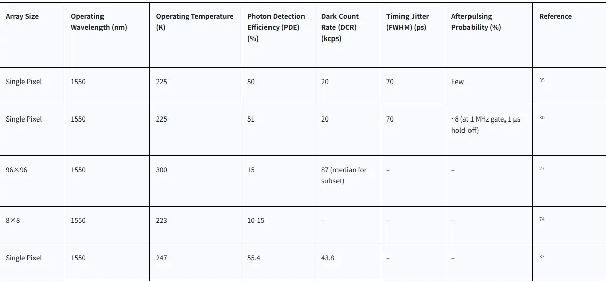
Photon Detection Efficiency (PDE) is a crucial performance metric for SPADs, representing the probability that an incident photon will be detected by the device. It is defined as the ratio of the number of detected photons to the total number of photons incident on the detector. InGaAs/InP SPADs have demonstrated impressive PDEs, with values reaching as high as 50% at a wavelength of 1550 nm when operated at a temperature of 225 K. Some research reports even indicate the achievement of higher PDE values under specific conditions. The PDE of an InGaAs SPAD is determined by two primary factors: the probability that an incident photon is absorbed within the InGaAs layer and the probability that a photogenerated carrier (typically a hole in InGaAs/InP SPADs) will trigger a self-sustaining avalanche process. Several factors can influence the PDE. The thickness of the InGaAs absorption layer plays a significant role, as a thicker layer generally increases the probability of photon absorption. The application of anti-reflection coatings on the detector surface can also enhance PDE by minimizing the loss of incident photons due to reflection. The applied excess bias voltage, which is the voltage above the breakdown voltage at which the SPAD is operated, also affects the PDE. Furthermore, the PDE of InGaAs SPADs is wavelength-dependent. For instance, the PDE might be higher for photons with wavelengths around 1 μm compared to those at 1550 nm. The operating temperature of the SPAD can also influence its PDE. The detailed design of the SPAD structure, including the incorporation of grading layers and charge layers within the semiconductor heterostructure, is critical for optimizing the electric field profile and thus the PDE. In some array designs, microlenses are integrated on top of each pixel to focus more light onto the active area, effectively increasing the PDE of the individual SPADs.
4.2 Dark Count Rate (DCR) and Noise Considerations
Dark Count Rate (DCR) is a critical parameter that characterizes the noise performance of a SPAD. It represents the rate at which spurious detection pulses occur in the absence of any incident light. Due to its narrower bandgap compared to silicon, InGaAs/InP SPADs generally exhibit a higher DCR. The DCR is strongly influenced by the operating temperature and the applied bias voltage. Cooling the SPAD to lower temperatures is a common and effective method to significantly reduce the DCR. Typical operating temperatures for InGaAs SPADs often range from 200 to 250 K. However, advancements in technology have led to the development of devices that can operate at room temperature with reasonably low DCRs. The generation of dark counts in SPADs primarily arises from thermal generation of charge carriers within the semiconductor material and from quantum tunneling mechanisms. It has been observed that increased doping concentrations in advanced CMOS technologies can sometimes lead to higher DCRs in integrated SPADs. To mitigate the DCR, various design strategies are employed, including the use of guard ring structures and the optimization of doping profiles within the SPAD. The DCR of a SPAD is often specified under particular operating conditions, such as at a specific photon detection efficiency and temperature. For a 96×96 InGaAs/InP SPAD array, a median DCR value as low as 87 kcps at room temperature has been reported for a subset of the pixels. For single-pixel InGaAs SPADs operated at lower temperatures, DCR values well below 1 kHz have been achieved.
4.3 Timing Jitter and Temporal Resolution
Timing jitter is a crucial performance characteristic of SPADs, quantifying the variation in the time interval between the arrival of a photon at the detector and the generation of the corresponding output pulse. This temporal uncertainty directly impacts the overall timing resolution of the detector. InGaAs SPADs are generally known for their fast response times and high temporal resolution, often achieving resolutions in the range of a few tens to hundreds of picoseconds. For instance, timing jitter values as low as 70 ps (full width at half maximum, FWHM) have been reported for InGaAs SPADs operating at 225 K , and some studies have demonstrated even lower jitter under specific conditions. The magnitude of the timing jitter can be influenced by the underlying CMOS technology used to fabricate the SPAD, with smaller depletion regions generally leading to lower jitter values. Techniques such as high-frequency sine wave gating have also been shown to achieve low timing jitter in InGaAs SPADs. High timing resolution is essential for a wide range of applications that rely on the precise measurement of photon arrival times, including Light Detection and Ranging (LiDAR) and Fluorescence Lifetime Imaging Microscopy (FLIM).
4.4 Afterpulsing Effects and Mitigation Strategies
Afterpulsing is a phenomenon that can occur in SPADs, where a detection event is followed by one or more spurious pulses occurring at a later time. These delayed false signals are typically caused by charge carriers that become trapped in the multiplication layer of the SPAD during a previous avalanche event. These trapped carriers can be released at a later time, potentially triggering another avalanche and resulting in a false photon detection. The probability of afterpulsing is generally reduced at room temperature compared to lower operating temperatures. One common strategy to mitigate afterpulsing is to apply a dead time, also known as a hold-off time, after each detected photon event. During this dead time, the SPAD is held at a bias voltage below the breakdown threshold, allowing any trapped carriers to be released without triggering a new avalanche. While longer dead times are effective in reducing afterpulsing, they can also limit the maximum rate at which the SPAD can detect and count photons. The use of active quenching circuits represents another effective approach to minimize afterpulsing. These circuits rapidly quench the avalanche current after a detection, which helps to reduce the number of carriers that become trapped in the first place, thereby lowering the probability of afterpulsing. Operating SPADs in a gated mode, where the bias voltage is periodically pulsed above the breakdown voltage for short durations, can also be beneficial in reducing afterpulsing. Furthermore, specialized SPAD designs, such as negative feedback avalanche diodes (NFADs), are engineered for free-running operation with inherently low afterpulsing probabilities. With the implementation of appropriate quenching techniques and hold-off times, the afterpulsing probability in InGaAs SPADs can be reduced to just a few percent.
4.5 Maximum Count Rate and Dynamic Range
The maximum rate at which a SPAD can accurately detect and count photons is fundamentally limited by its dead time and the recovery time of its associated circuitry. A shorter dead time allows the SPAD to be reset more quickly, enabling it to detect subsequent photons at a higher rate. For instance, free-running InGaAs/InP SPADs utilizing GHz gating techniques have demonstrated impressive count rates reaching up to 500 Mcount/s. When an 8×8 SPAD array is operated in a combined mode, effectively functioning as a single large-area detector, it has the potential to achieve a maximum photon detection rate that is 64 times higher than that of an individual SPAD pixel. Dynamic range, which refers to the ratio between the maximum and minimum detectable signal levels, is another important performance characteristic. SPADs are known for offering a high dynamic range, allowing them to detect both very faint light signals and relatively strong signals without saturation. The inherent non-linear response of SPADs to light contributes to their wide dynamic range. Furthermore, some SPAD systems are designed to operate in a dual mode, switching between a linear mode and the Geiger mode, which can further extend the overall dynamic range of the detector.
4.6 Impact of Operating Temperature
The operating temperature has a significant impact on the performance characteristics of InGaAs SPAD arrays. Generally, lowering the operating temperature leads to a reduction in the dark count rate. The photon detection efficiency can also be influenced by the temperature at which the SPAD is operated. The probability of afterpulsing, a phenomenon where a spurious detection occurs after a genuine photon detection, can also be affected by temperature. In some cases, afterpulsing probability might be reduced at higher temperatures due to faster release times of trapped charge carriers. The breakdown voltage of the SPAD, which is the reverse bias voltage at which the avalanche process initiates, can also exhibit a temperature coefficient, meaning it changes with temperature. For InGaAs SPADs, the optimal operating temperature is often found to be in the range of 200 to 250 K. However, advancements in device design and fabrication have resulted in some InGaAs SPADs that can operate at room temperature with acceptable levels of performance. Another important performance parameter, the Noise Equivalent Power (NEP), which represents the minimum detectable optical power, can decrease significantly when the operating temperature of the InGaAs SPAD is lowered.
Table 1: Typical Performance Parameters of InGaAs SPAD Arrays
Applications of InGaAs 8×8 Array SPADs
5.1 Light Detection and Ranging (LiDAR) for Autonomous Systems and Mapping
InGaAs SPAD arrays, including the 8×8 configuration, are extensively utilized in Light Detection and Ranging (LiDAR) systems for generating high-resolution three-dimensional maps of their surroundings. Their exceptional sensitivity to single photons allows them to detect even the faintest reflections of emitted laser pulses, making them particularly well-suited for operation in low-light environments and enabling long-range detection capabilities. LiDAR systems employing SPAD arrays typically measure the distance to objects by precisely determining the time it takes for short laser pulses to travel to the target and return to the detector, a technique known as time-of-flight measurement. The use of SPAD arrays in LiDAR offers the advantage of higher data acquisition throughput and improved noise performance compared to single-pixel detectors. In many LiDAR applications, particularly those involving autonomous systems, eye-safe laser wavelengths in the vicinity of 1550 nm are preferred for safety reasons, and InGaAs SPADs exhibit excellent performance at these wavelengths. Research efforts have demonstrated the use of 8×8 InGaAs SPAD arrays for short-range LiDAR sensors, highlighting their potential in this domain. Furthermore, to enhance the quality of the 3D reconstructions obtained from SPAD array data, sophisticated computational imaging algorithms are under development. These algorithms aim to address challenges such as motion blur in dynamic scenes and to increase the effective spatial resolution of theacquired data.
5.2 Quantum Communication and Quantum Key Distribution (QKD)
InGaAs SPAD arrays play a pivotal role in the field of quantum communication and quantum key distribution (QKD). They are essential components in experiments involving single-photon sources, quantum entanglement, and various other quantum optics applications. InGaAs/InP SPADs are particularly well-suited for single-photon detection in the near-infrared spectral region, which is crucial for quantum communication systems that utilize optical fibers, as these wavelengths experience lower transmission losses. SPAD arrays are employed to detect and measure individual photons, which serve as the fundamental carriers of quantum keys in secure communication protocols. The use of arrays in QKD systems can lead to increased data transmission rates. Notably, high-frequency gated InGaAs/InP SPADs are critical components in the development and deployment of long-range quantum communication networks.
5.3 Fluorescence Lifetime Imaging Microscopy (FLIM) and Biomedical Imaging
InGaAs SPAD arrays are increasingly finding applications in biomedical imaging, particularly in techniques like Fluorescence Lifetime Imaging Microscopy (FLIM). SPAD cameras, by virtue of their array architecture, offer a significant increase in overall photon throughput compared to traditional scanned detection systems used in FLIM. This enhanced throughput can simplify the experimental setup required for FLIM and lead to increased imaging frame rates. Due to their single-photon sensitivity and precise timing capabilities, SPAD arrays can accurately capture the fluorescence decay times of fluorescently labeled molecules, providing researchers with detailed insights into underlying biological mechanisms. In confocal microscopy, SPAD arrays enhance light collection efficiency, resulting in sharper and brighter images that can also provide functional information about molecular interactions and the cellular environment. Furthermore, InGaAs SPAD arrays are being explored for use in time-of-flight positron emission tomography (ToF-PET), a medical imaging modality used for diagnostics. They also find applications in Raman spectroscopy for biomedical imaging purposes. Emerging applications include the potential use of InGaAs SPAD arrays in wireless fluorescence capsule endoscopy for medical diagnosis.
5.4 High-Speed Imaging and Light-in-Flight Applications
The unique characteristics of SPAD arrays, including their single-photon sensitivity and fast response times, make them ideally suited for high-speed imaging applications. SPAD cameras can achieve high frame rates while operating with a global shutter and exhibiting zero readout noise. This combination of features enables the imaging of extremely fast phenomena even under very low light conditions. Moreover, the high temporal resolution of SPAD arrays allows for the fascinating capability of imaging light as it propagates through space, a technique often referred to as light-in-flight imaging.
5.5 Other Emerging Applications (e.g., Spectroscopy, Quantum Optics)
Beyond the primary applications discussed above, InGaAs SPAD arrays are finding increasing use in a diverse range of other emerging fields. These include various forms of spectroscopy, where their high sensitivity and broad spectral range are advantageous. In the domain of quantum optics, SPAD arrays with low crosstalk are crucial for experiments such as quantum random number generation. Their sensitivity to weak light also makes them valuable for industrial applications like wafer inspection and particle sizing. In biomedical research, they are utilized in flow cytometry for high-throughput cell analysis and in confocal microscopy for advanced cellular imaging. Other applications include optical tomography, quantum computing, single molecule analysis, astronomy, plasma research, nuclear physics, high energy physics, night vision, non-destructive testing of materials, and eye-safe laser-based systems. Furthermore, InGaAs SPAD arrays are being explored for free-space optical communication, optical coherence tomography, imaging in high radiation environments, augmented reality interfaces, gesture recognition systems, environmental sensing, and as radiation detectors.
Recent Advancements and Future Trends in InGaAs SPAD Array Technology
6.1 Progress in Achieving Higher PDE and Lower DCR
Ongoing research and development in InGaAs SPAD array technology are continuously pushing the boundaries of performance. Significant progress is being made in achieving higher Photon Detection Efficiencies (PDEs) and lower Dark Count Rates (DCRs). This is being accomplished through continuous optimization of SPAD structures, including the use of thicker InGaAs absorption layers to capture more incident photons, the implementation of novel doping profiles such as double-well diffusion to tailor the electric field within the device, and the incorporation of reflective layers and microlenses to enhance light collection. Advancements in semiconductor fabrication techniques and improvements in the quality of the InGaAs material itself are also contributing to the realization of lower dark count rates, even at relatively higher operating temperatures. The strategic use of guard ring structures and the careful design of charge layers within the SPAD heterostructure play a crucial role in controlling the electric fields and minimizing unwanted noise, leading to lower DCRs. Researchers are also exploring alternative material systems, such as InGaAs/AlGaAsSb, as promising candidates for developing passively-cooled SPADs that can operate efficiently at room temperature without the need for thermoelectric coolers. Furthermore, continuous improvements are being made in reducing afterpulsing effects through the implementation of fast active quenching circuits that rapidly terminate the avalanche process and through optimized management of the dead time after each detection event.
6.2 Integration with CMOS Technology for Enhanced Functionality
A significant trend in the advancement of InGaAs SPAD array technology is the increasing integration of these detectors with complementary metal-oxide-semiconductor (CMOS) technology. This integration enables the incorporation of advanced functionalities directly onto the same chip as the detector array, such as in-pixel Time-to-Digital Converters (TDCs) for precise timing measurements, active quenching circuits to rapidly reset the SPAD after a detection, and sophisticated digital signal processing capabilities. CMOS technology provides a mature and cost-effective platform for the development of large digital arrays that integrate both the detectors and the necessary control and readout circuits, allowing for the tailoring of these sensors to meet the specific needs of various applications. Techniques like three-dimensional (3D) stacking architectures are being employed to further enhance the photosensitivity of the SPADs and to enable the integration of even more complex electronic circuits in a compact footprint. This high level of integration facilitates features such as fast gating of the SPADs for time-resolved measurements and on-chip histogram processing for advanced data analysis. Researchers are also actively exploring the monolithic integration of InGaAs SPADs with silicon-based photonic integrated circuits, which could lead to even more compact and efficient optoelectronic systems.
6.3 Development of Larger and Higher-Resolution SPAD Arrays
A clear trend in the evolution of InGaAs SPAD array technology is the development of larger format arrays with an increasing number of pixels, leading to higher spatial resolution. Examples include arrays with resolutions of 96×96 , 512×128 , 512×512 , 256×64 , 32×32 , 128×32 , and 64×64 pixels. Significant efforts are focused on increasing the density of pixels within the array by reducing the size of individual pixels and the pitch between them. The availability of larger and higher-resolution SPAD arrays directly translates to enhanced performance in applications such as LiDAR and imaging, providing a wider field of view and the ability to capture finer spatial details.
6.4 Novel Applications Driven by Technological Improvements
The continuous advancements in the performance and integration capabilities of InGaAs SPAD arrays are enabling the exploration of entirely new and previously unfeasible applications. These emerging applications highlight the transformative potential of this technology across a wide range of fields. One such area is non-line-of-sight (NLOS) imaging, where SPAD arrays are being investigated for their ability to reconstruct images of objects hidden from direct view. The high sensitivity and timing resolution of these arrays are also being leveraged for underwater 3D imaging applications. Furthermore, InGaAs SPADs are being explored for integration into consumer electronics, such as laser autofocus solutions for smartphones. Their potential for use in eye-tracking systems for augmented and virtual reality interfaces is also being investigated. Other novel applications include high-speed underwater imaging, free-space optical communication for secure data transmission, advanced spectroscopy techniques like ultra-fast Raman spectroscopy for material analysis, and their use in radiation detection and high-energy physics experiments.
Conclusion
InGaAs 8×8 Array Single-Photon Avalanche Diodes represent a significant advancement in the field of photon detection, offering a powerful combination of high sensitivity capable of detecting individual photons, fast timing resolution in the picosecond range, and the benefits of an array format allowing for parallel data acquisition. These unique characteristics have positioned InGaAs 8×8 Array SPADs as enabling technologies in a wide array of critical applications, most notably in Light Detection and Ranging (LiDAR) systems for autonomous vehicles and high-resolution mapping, as well as in the burgeoning field of quantum communication and secure Quantum Key Distribution (QKD). Furthermore, their exceptional sensitivity and temporal precision make them invaluable tools in biomedical imaging techniques such as Fluorescence Lifetime Imaging Microscopy (FLIM) and Positron Emission Tomography (PET). The ability to capture high-speed phenomena and even visualize the propagation of light itself underscores their significance in advanced scientific research. The field continues to witness rapid advancements, with ongoing research focused on achieving even higher photon detection efficiencies, reducing intrinsic noise levels, and seamlessly integrating these arrays with sophisticated CMOS technology for enhanced functionality. The trend towards developing larger and higher-resolution arrays promises to further expand their capabilities and open up new horizons in various applications. As the technology matures, InGaAs 8×8 Array SPADs are poised to play an increasingly crucial role in a wide spectrum of scientific, industrial, and consumer applications, driving innovation and enabling breakthroughs in diverse fields.