


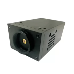
Introduction and Overview: The OP501C InGaAs 4×4 Single-Photon Avalanche Diode (SPAD) Array is a compact photodiode module engineered for ultra-sensitive light detection in the near-infrared (NIR) spectrum. It comprises a 4×4 array of indium gallium arsenide SPAD pixels (16 total), along with integrated active quenching circuits, a thermoelectric cooler, and signal processing electronics. Each SPAD pixel can register individual photons, producing a fast electrical pulse for each detected photon event. By combining multiple SPADs into a 16-pixel array, the OP501C functions as a multi-channel single-photon detector, effectively a small “single-photon camera” with extremely high sensitivity. The module is designed to detect weak optical signals at the single-photon level with high timing resolution, making it suitable for demanding applications like long-range laser ranging, quantum optical communication, and time-resolved imaging. Notably, the OP501C achieves this performance in a self-contained unit roughly 75×50×28 mm in size, simplifying integration into larger systems.
Key Features and Specifications of the OP501C
The OP501C detector module’s design centers on an InGaAs SPAD focal plane array with 4×4 = 16 pixels, each operating in Geiger mode (biased above avalanche breakdown to detect single photons). The pixels are arranged on a 100 µm pitch (center-to-center), with an active area of roughly 80–85 µm per pixel and small gaps (~20 µm) between them. This format yields a total photosensitive area of about 0.4 × 0.4 mm for the array. The key performance specifications are summarized below:
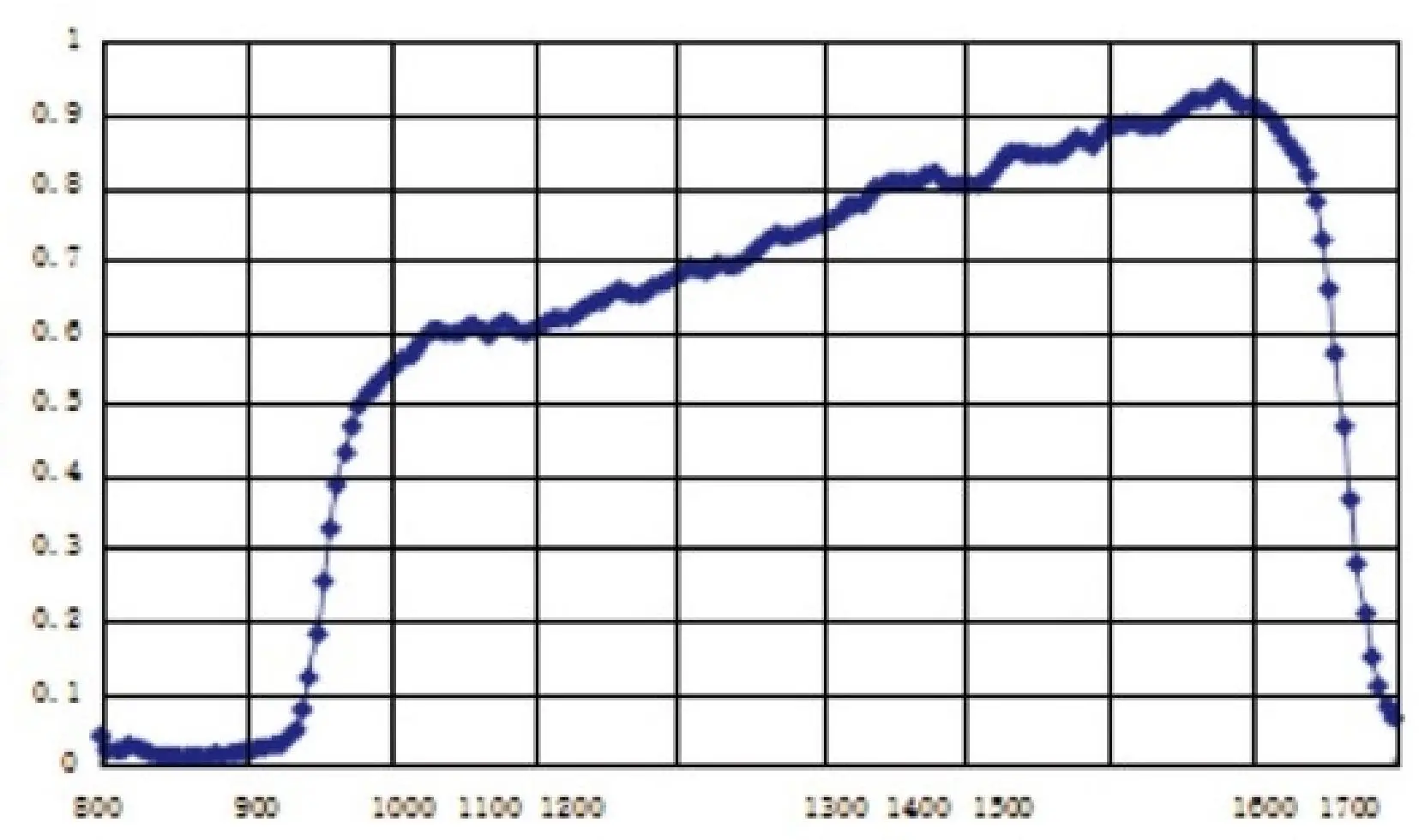
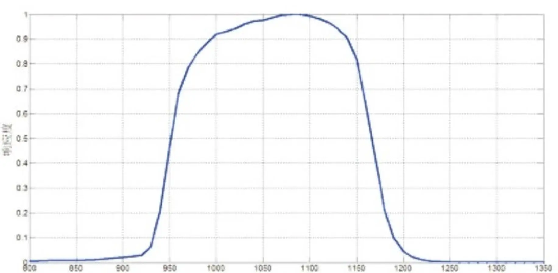
- Spectral Response: Sensitive to NIR wavelengths from 1000 nm up to ~1650 nm, covering the important telecom bands at 1310 nm and 1550 nm. The peak photon detection efficiency (PDE) is around 15% at 1.57 µm (typical) when the device is cooled to ~–30 °C. Figure 1 shows a representative spectral response curve: the InGaAs SPAD pixels maintain >10% efficiency across much of the 1000–1650 nm range, with a broad plateau through the telecom region and roll-off near the band edges. By tailoring the InGaAs/InP structure (or using InGaAsP layers), the spectral response can be optimized for specific bands (Fig. 1 vs Fig. 2) as discussed later.
- Single-Photon Sensitivity: The SPAD pixels are capable of detecting extremely weak signals – each photon absorbed in a pixel triggers a discrete output pulse. At the specified operating bias (set for ~10% PDE), each pixel’s dark count rate (false counts from thermal carriers) is on the order of 10 kHz when cooled. This low dark noise is achieved via the built-in thermoelectric cooling and high-quality InGaAs material. The afterpulsing probability (spurious second pulses from trapped charge) is specified at ~20% under those conditions, a typical value for InGaAs SPADs. The module provides a fast output pulse for each detected photon, with amplitude about 3.3 V (TTL logic level) and configurable pulse width. Each pixel operates independently, delivering its own pulse output without crosstalk (aside from minimal electrical/optical crosstalk that is mitigated by design).
- Integrated Cooling and Quenching: The OP501C’s housing includes a thermoelectric cooler (TEC) that actively refrigerates the SPAD array to around –30 °C during operation. This cooling dramatically suppresses thermal dark noise, improving signal-to-noise for single-photon detection. The module also incorporates active quenching circuits for each pixel, ensuring that after a photon-triggered avalanche, the diode is rapidly reset (quenched) within a few nanoseconds to be ready for the next photon. A fixed dead time (on the order of 0.8 µs) is enforced after each detection to allow the pixel to recover and to reduce afterpulsing. These support circuits (cooler and quench circuitry) are built-in, simplifying use – the end user does not need to separately provide bias gating or cooling, as would be required for a bare SPAD device.
- Electrical and Interface Specs: The module runs on a single +5 V DC supply (~3 A typical draw, or ~15 W power consumption when the TEC is active). It provides a high-density electrical connector for the 16 channel outputs (one TTL pulse output per pixel), as well as a UART serial interface for control and configuration. There are also two SMA connectors on the module: one for a synchronization input and one for a synchronization output. These allow an external trigger or clock to synchronize the SPAD operation (for example, gating the detector in sync with a laser pulse) and/or to output a timing signal. The operating ambient temperature range is specified from –40 °C to +55 °C, indicating the module is suitable for use in varied environmental conditions. The device weighs ~180 g and measures roughly 75 × 50 × 28 mm, housed in a metal enclosure with mounting points and an optical aperture at the front.
In summary, the OP501C offers a turnkey single-photon detection solution in the NIR: a 16-pixel array with each pixel having ~10–15% efficiency for 1.5 µm photons, cooled for low noise (~10 kHz dark counts), and delivering TTL-level pulse outputs. This combination of features – multi-pixel capability, integrated cooling/quenching, and high sensitivity – makes it a unique module for advanced photonics applications that require detection of extremely weak optical signals.
InGaAs SPAD Technology Principles
SPAD Operation (Geiger-Mode Avalanche): The core of the OP501C is an array of InGaAs single-photon avalanche diodes, each operated in Geiger mode. In normal APD operation below breakdown, a photodiode produces a proportional current to incident light. In Geiger mode, however, the diode is biased above its breakdown voltage, so that the absorption of a single photon can trigger a self-sustaining avalanche of carriers. Essentially, each SPAD pixel is a tiny p-n junction engineered with a specialized structure: an InGaAs absorption layer that efficiently absorbs NIR photons, bonded to an InP multiplication layer that provides a high electric field for avalanche multiplication. When a photon enters the diode and is absorbed in the InGaAs region, it generates an electron-hole pair. The built-in electric field sweeps one of these carriers into the high-field InP layer, where it gains enough energy to ionize the lattice, creating a cascade of additional carriers (impact ionization). This avalanche multiplication yields a large current spike from a single photon trigger. The device thus outputs a discrete electrical pulse indicating the arrival of one photon (with no proportionality to photon energy or number – it’s a digital on/off response). A SPAD can be thought of as a photon-triggered switch: once triggered, it stays conducting (in avalanche) until the electronics actively quench the event.
Quenching and Reset: In a Geiger-mode SPAD, after an avalanche is triggered, it must be stopped quickly to ready the diode for the next photon and to protect it from damage. The OP501C integrates a fast quenching circuit for each pixel that detects the onset of an avalanche and rapidly reduces the bias across that SPAD, terminating the current. This can be done either passively (with a resistor that drops voltage as current flows) or actively (with a transistor that quickly pulls the bias down). The OP501C’s design uses a combination of active and passive quenching on each channel. Quenching typically occurs within a few nanoseconds of the avalanche start, after which the bias is held below breakdown for a fixed dead time (to allow charge traps to clear). After this dead time (e.g. ~0.8 µs), the bias is restored above breakdown and the SPAD is armed to detect the next photon. Each avalanche event thus produces a fixed-width pulse output and then a brief blind period. The integrated quenching ensures each pixel operates independently and in free-running mode (not requiring an external gating signal for basic operation). This means the array can continuously detect photons on all pixels in parallel, with each pixel asynchronously generating pulses whenever photons are incident.
InGaAs/InP Structure and Material Considerations: InGaAs SPADs are typically implemented as separate absorption and multiplication (SAM) or separate absorption, grading, charge, and multiplication (SAGCM) structures. The OP501C’s SPAD array follows this approach. The Indium Gallium Arsenide (In0.53Ga0.47As) layer (lattice-matched to InP) is used as the photon absorption region. InGaAs has a bandgap of ~0.75 eV, corresponding to a cutoff wavelength of ~1.67 µm, which covers the OP501C’s 1000–1650 nm sensitivity range. Beneath (or above) the InGaAs, a layer of Indium Phosphide (InP) acts as the avalanche multiplication region. InP has a wider bandgap (~1.34 eV) and is transparent to the NIR photons, so virtually all the light is absorbed in the InGaAs layer but the avalanche takes place in the InP layer. This separation is crucial: it allows optimization of the absorption layer (for high quantum efficiency) independently from the multiplication layer (for high avalanche gain). Additionally, modern InGaAs SPAD designs include a grading layer of InGaAsP between the InGaAs and InP. This InGaAsP layer has a graded composition to smooth the transition in bandgap (from 0.75 eV to 1.34 eV) and lattice, reducing carrier trapping at the heterointerface. It also subtly shapes the spectral response – for example, by adjusting the InGaAsP composition, manufacturers can shift the peak sensitivity or cutoff wavelength (Fig. 2 shows an example spectral curve for a particular InGaAsP composition). The OP501C datasheet in fact provides two spectral curves, one labeled “InGaAs” and one “InGaAsP,” indicating the device’s response and possibly the material mix used.
Performance Trade-offs: InGaAs SPAD technology presents some inherent challenges compared to silicon SPADs. InGaAs devices typically have higher dark count rates and afterpulsing due to greater material defect densities and deep-level traps in III-V materials. To mitigate this, the OP501C (like most InGaAs SPAD modules) uses thermal cooling and can employ gated operation if needed. Cooling the SPAD to –30 °C or below suppresses thermal carrier generation exponentially – the OP501C’s ~10 kHz dark count at –30 °C would be orders of magnitude higher at room temperature. Additionally, operating the SPAD in gated mode (bias above breakdown only during a short window when a photon is expected) can dramatically reduce afterpulsing by giving traps more time to empty between avalanches. The OP501C provides a sync input that could be used to implement such gating for applications like periodic lidar pulses or clocked quantum communications. However, in many cases the module is used free-running, relying on its short dead time and cooling to keep afterpulse and dark counts manageable. Each pixel’s timing jitter (temporal uncertainty in detecting a photon) is on the order of a few hundred picoseconds (exact jitter not explicitly stated, but InGaAs SPADs typically achieve ~100–500 ps FWHM timing resolution). This is sufficient for time-of-flight ranging and coincidence timing in most applications, though not as fast as some specialized single-pixel detectors (e.g. ID Quantique’s detectors can reach ~80 ps with dedicated timing electronics).
In summary, the OP501C leverages the fundamental InGaAs/InP SPAD principle: a separated absorption and multiplication region to detect single NIR photons with avalanche gain. Its on-board quenching circuits and cooler are critical enabling technologies that allow these SPADs to operate stably and with low noise in the field. Understanding this device physics background clarifies why the OP501C can achieve high sensitivity (thanks to InGaAs absorption), while managing noise (thanks to cooling and circuit design), and why its performance parameters (PDE ~15%, dark counts ~10^4/s) are in line with the state-of-the-art for InGaAs SPADs.
InGaAs and InGaAsP Materials: Spectral Response and Cooling Requirements
The choice of InGaAs (and related alloys) as the photosensitive material is what grants the OP501C its near-infrared capability. Pure InP diodes are not sensitive beyond ~1.0 µm, and silicon SPADs cease to be efficient past ~1.1 µm due to bandgap limitations. By using In0.53Ga0.47As (which is lattice-matched to InP substrates), detectors can cover the telecom bands (1260 nm and 1550 nm) and even up to the eye-safe 1.6 µm region. The spectral response behavior of these InGaAs SPADs is governed by the absorption coefficient of the material, which increases toward shorter wavelengths (until near the bandgap edge). Figure 1 illustrates a typical PDE vs. wavelength: the efficiency rises from around 0.9–1.0 µm (as photons get above the bandgap energy threshold) to a peak in the 1.2–1.3 µm range, and then gradually declines by 1.6–1.7 µm as the absorption in InGaAs weakens near its cutoff. In practice, the OP501C achieves a relatively flat efficiency ~10–15% across 1.0–1.6 µm by biasing the diodes sufficiently high. The inclusion of an InGaAsP grading layer can further smooth the spectral response. For instance, an InGaAsP layer tuned closer to 1.3 µm bandgap can make the detector slightly more efficient around 1310 nm (Fig. 2 shows a pronounced peak around that wavelength), albeit at the cost of sensitivity at the extreme 1.6 µm end. Manufacturers balance these trade-offs depending on target application – some SPADs might be optimized for 1550 nm peak (for LIDAR at that wavelength), others for 1064 nm (Nd:YAG laser applications) using a different InGaAsP composition.
Cooling Requirements: Cooling is virtually mandatory for InGaAs SPADs in low-light applications. At room temperature, InGaAs diodes suffer from high dark currents and high rates of spontaneous avalanches (dark counts) due to thermal excitation of carriers across the small bandgap (0.75 eV). By cooling the detector to –20 °C, –30 °C or even lower, the thermal generation rate is dramatically reduced. The OP501C’s TEC holds the array at about –30 °C, at which point a typical pixel with PDE ~10% has a dark count rate ~10 kHz. If the device were run uncooled at 25 °C, that dark count could easily be in the hundreds of kHz or more, effectively swamping single-photon signals. In laboratory settings, some InGaAs SPAD detectors are cooled to –80 °C or –100 °C (using multi-stage TECs or liquid nitrogen) to push dark counts down to just a few counts per second. The OP501C’s cooling is a single-stage thermoelectric suited for field use, striking a balance between performance and practicality (15 W power draw is reasonable for many setups). It brings the dark count into a manageable range for applications like lidar or quantum comms, where some false counts can be tolerated and filtered out. Users should be aware that the module will dissipate heat (via the TEC) and may require a heat sink or airflow to maintain the cooling performance – the specified 15 W power consumption is largely for pumping heat from the cold SPAD array to the ambient.
It’s also worth noting that cooling helps reduce afterpulsing. Afterpulses are triggered by charge carriers trapped in lattice defects during an avalanche that later release and cause a new avalanche. At lower temperatures, carriers have less energy and are less likely to get trapped, plus the longer carrier lifetime in traps might actually increase afterpulse if not gated. There is a complex interplay: typically, moderate cooling (down to –30 or –50 °C) lowers dark noise significantly without dramatically increasing trap lifetime, yielding an overall reduction in afterpulse rate. The OP501C’s afterpulse probability ~20% (at 10% PDE) is measured under cooled conditions, and this will worsen if the detector warms up. In critical timing applications, additional measures like gating the bias (using the sync input to only arm the SPADs at certain times) can further mitigate afterpulsing by giving traps more time to empty between avalanches.
InGaAsP vs InGaAs Material Use: Why mention InGaAsP at all for a SPAD? As introduced, InGaAsP can serve as a grading or absorption layer with intermediate bandgap. Some SPAD designs use an InGaAsP absorption layer (instead of InGaAs) to target wavelengths around 1.06–1.1 µm (where InGaAs would be overkill and just add dark noise). InGaAsP can be formulated with a bandgap corresponding to ~1.06 µm, which still allows detection of 1.06 µm photons but with significantly lower dark current than an InGaAs layer (since its bandgap is larger). For example, a SPAD intended for detecting a Nd:YAG 1064 nm laser might use InGaAsP so that photons just above 1064 nm are absorbed, but longer wavelengths (like 1550 nm) are not, reducing background sensitivity. In the case of the OP501C, the mention of an “InGaAsP spectral response curve” suggests the device may incorporate a layered structure where both materials play roles (perhaps a graded structure). It could also be informational, showing how the device behaves across materials. Regardless, the key point is that InGaAs/InP technology is what enables the broad NIR sensitivity, and the integrated cooler is what makes it usable for single-photon counting by taming the noise.
In summary, the OP501C’s material stack and cooling are carefully designed for maximum sensitivity in the NIR with minimal noise. InGaAs provides the light absorption up to 1.65 µm, InP provides gain, and cooling plus material engineering (like InGaAsP layers and guard rings to prevent edge breakdown) ensure that the detector can operate in a stable Geiger mode. Users should operate the module with its cooler active and consider maintaining the recommended –30 °C setpoint for best results, especially if aiming for the specified PDE and dark count levels.
Typical Application Domains of the OP501C
Single-photon detectors in the 1.0–1.6 µm range are critical enabling components for a variety of advanced technologies. The OP501C, with its 16-pixel NIR SPAD array, is positioned for use in several key application domains:
- Quantum Communication (QKD and Quantum Optics): Secure quantum communication protocols, such as Quantum Key Distribution (QKD), often transmit single photons (or faint laser pulses) over fiber or free-space in the telecom bands. InGaAs SPADs are the workhorse detectors for these systems, especially for free-running or gated detection at 1310 nm and 1550 nm. The OP501C could serve as a multi-channel single-photon receiver in a QKD system – for example, one module could replace multiple single-SPAD units by using different pixels for different polarization states or time-bin channels. Each pixel’s timing resolution (sub-nanosecond) is sufficient for the nanosecond-scale time slots used in QKD protocols. Beyond QKD, quantum optics experiments (entanglement swapping, teleportation, quantum Lidar, etc.) can benefit from an array of detectors. For instance, in a quantum entanglement experiment, an OP501C could detect coincident single photons across multiple spatial modes or channels simultaneously. Traditional setups might require multiple separate detectors like ID Quantique’s ID210/230 modules; a single OP501C can provide 16 detectors in one package, albeit with somewhat higher per-detector noise than the ultra-low-noise lab modules. The convenience of a multi-pixel module is especially attractive for research setups that need many detectors (e.g. multi-photon coincidence measurements) without the complexity of synchronizing many separate devices.
- Laser Ranging and LiDAR: One of the primary advertised uses of the OP501C is long-distance laser ranging and optoelectronic radar (which is essentially another term for laser-based radar or LiDAR). In this context, the detector is used to measure the time-of-flight of laser pulses reflecting off distant targets. Because the returned signal from far-away or low-reflectivity targets can be just a few photons, SPADs are ideal sensors for eye-safe LiDAR systems at 1550 nm. A 4×4 SPAD array can be used in a scanning LiDAR, where each pixel covers a portion of the field or sequential shots are taken with different pixels, or in a flash LiDAR configuration where a 4×4 “frame” of depth information is captured at once (though 4×4 is a coarse image, it could still discern multiple objects or spatially separated returns). The OP501C’s pixels operate in parallel, so in a LiDAR application, you could obtain multiple distance readings simultaneously – for example, if multiple targets are at different angles, different pixels will detect their respective returns. The module’s synchronization features (the SMA trigger ports) are very useful here: one can input a sync signal tied to the outgoing laser pulse so that each SPAD pixel is activated or at least time-tagged relative to the emission. The low timing jitter (hundreds of ps) corresponds to a few centimeters of range precision, and with appropriate calibration, sub-centimeter resolution can be attained by averaging. The modest array size (4×4) is not meant to form a high-resolution image like a camera; instead it might increase the collective aperture (16 pixels can cover a larger area or multiple fibers) or provide minimal imaging to distinguish, say, an object’s center vs edges. Long-range LiDAR systems (for aerospace or mapping) sometimes employ such SPAD arrays for their unparalleled sensitivity – for example, 32×32 InGaAs SPAD arrays have been used for flash lidar from aircraft and even for planetary landing prototypes. The OP501C is a smaller-scale, commercially available version suitable for experimental and lower-channel-count systems.
- Optical Space Communication: In deep-space optical communication or satellite-to-ground laser links, the path loss is so high that single-photon detection is often required on the receiver end. InGaAs SPADs have been used in optical communication terminals to receive faint pulses from spacecraft tens of thousands of kilometers away. The OP501C, with its NIR sensitivity and multiple pixels, could function as part of a receiver that not only detects the presence of photons but also helps with spatial acquisition and tracking. For example, a 4×4 array at the focus of a telescope can act as a tracking sensor: if the incoming beam wanders due to atmospheric turbulence or pointing errors, different SPAD pixels will click. By monitoring which pixel(s) register photons, the system can actively adjust pointing or feed that information to a fine steering mirror. Meanwhile, one or more of the pixels can be designated as the primary data receiver. The sync output of the OP501C could provide a timing signal to communication logic to timestamp each photon for data decoding. Additionally, having multiple pixels helps in background discrimination – some pixels could monitor the background light level (starlight or ambient) while others look at the signal, enabling adaptive noise cancellation. The module’s lightweight, compact form factor is advantageous for space or airborne payloads where size, weight, and power (SWaP) are at a premium.
- Biomedical Imaging and Sensors: The near-infrared window of 1000–1700 nm is increasingly important in biomedical imaging because tissue has reduced scattering and absorption in this range (often called the NIR-II window). InGaAs SPADs like OP501C open up single-photon detection for techniques such as time-resolved fluorescence imaging, diffuse optical tomography, and biomedical LiDAR. For example, in fluorescence lifetime imaging microscopy (FLIM) or spectroscopy, a pulsed NIR laser might excite dye molecules in tissue and the extremely weak NIR fluorescence is detected and timed by SPADs to compute lifetimes. In one scenario, an array of SPADs can allow parallel acquisition of multiple points on a sample or multiple wavelength channels (by putting different filters in front of different pixels). The OP501C’s timing resolution (<1 ns) is adequate for many fluorescence lifetime measurements (which often involve lifetimes of a few nanoseconds or more). Another example is time-of-flight diffuse optical tomography – sending short laser pulses into tissue and detecting the faint, scattered return light. An array of SPADs can collect data from multiple source-detector positions at once, improving imaging speed for, say, brain functional imaging or small animal imaging. Additionally, the OP501C could serve in a biomedical LiDAR context: for instance, measuring distances inside the eye or within blood vessels using a catheter with an optical probe. The high sensitivity allows detection with minimal light dose, which is critical for safety in medical diagnostics. One more application is in remote biosensing – e.g., using a NIR laser to detect heart rate or blood oxygenation from the faint reflections on skin; a SPAD can pick up the tiny modulations at the single-photon level. In all these cases, the use of NIR wavelengths penetrates deeper into tissue, and single-photon sensitivity allows working at low powers for safety.
- Optoelectronic Radar and Laser Warning Systems: The term optoelectronic radar often refers to active laser sensors used in military or aerospace contexts for detection and ranging. The OP501C can be the sensor in a laser warning receiver, which is a device that detects incoming laser signals (for example, an adversary’s rangefinder or targeting laser) to alert the platform of a threat. Such systems require extremely high sensitivity because the scattered or stray photons from a distant laser designator are very few by the time they reach the sensor. A SPAD array can sense a nanosecond laser pulse even if only a handful of photons hit the detector】. With a 4×4 array, the system can also get a rough angle-of-arrival by comparing which pixel or quadrant sees the strongest signal, helping to localize the threat source. The fast response (<ns) means even very short laser pulses will be detected reliably. Another emerging field is photon-counting passive imaging or quantum lidar, where one uses ambient light or extremely low-power illumination and relies on counting individual photons reflected from objects to form an image or make a distance measurement. The OP501C could be used as the detector in a prototype passive imaging system operating in moonlight or starlight conditions (which have more NIR content than visible). Its 16 pixels could perform simple imaging or be combined with scanning to build up a higher resolution picture. In general, the combination of single-photon sensitivity + multiple apertures (pixels) gives a lot of flexibility for sensing and detection in low-light scenarios.
Across these applications, a common theme is that the OP501C provides a ready-to-use, multi-channel single-photon detector in a band (NIR) that is otherwise challenging for detectors. Before modules like this, engineers often had to resort to single-element InGaAs SPAD modules (and use several of them for multiple channels) or much more complex systems like superconducting nanowire detectors (which require cryogenics). The OP501C fills a niche for a practical, field-deployable NIR single-photon detector array that can be used in both R&D and in applied systems for sensing and communication.
Market Positioning and Comparison to Similar Products
InGaAs SPAD arrays are a specialized technology with only a few manufacturers and products available. The OP501C is notable as a commercially available 4×4 SPAD module, and understanding its market positioning is aided by comparing it to offerings from other leading players in single-photon detection. Here we consider similar or relevant products/technologies from Hamamatsu Photonics, ID Quantique, and Princeton Lightwave (as well as their successors):
- Lontenoe OP501C vs. Hamamatsu:Hamamatsu Photonics (Japan) is a renowned photonics company with expertise in photodiodes and imagers. Hamamatsu has indeed pursued InGaAs SPAD arrays in research – notably, they developed a 32×32 pixel InGaAs SPAD camera in collaboration with Japanese research institutions for flash LiDAR and planetary landing applications. That prototype had a 100 µm pixel pitch (like OP501C) and later versions achieved 55 µm pitch, showing Hamamatsu’s progress in miniaturizing pixels. However, as of the mid-2020s, Hamamatsu does not offer a multi-pixel InGaAs SPAD module as a standard product. They do provide related components – for instance, linear InGaAs APD arrays for spectroscopy and single-pixel SPAD modules (like the C12700 series, though those are typically Si SPADs or PMTs, and if InGaAs, they are one-pixel units). If a customer needs a 4×4 or similar InGaAs SPAD array, Hamamatsu could potentially develop a custom solution, but it’s not off-the-shelf. Therefore, the OP501C, produced by Lontenoe (and partners like EIPEKS), stands out as one of the few ready-made options for a 16-channel NIR SPAD detector. Hamamatsu’s research implies that in the future they might commercialize larger SPAD arrays (they have a strong track record in silicon multi-pixel photon counters, for example). But currently, an engineer or researcher wanting a module today would likely find OP501C or similar from smaller specialized firms, rather than a catalog item from Hamamatsu. In terms of performance, Hamamatsu’s 32×32 prototype reportedly had good uniformity and possibly integrated readout, but specifics like PDE and dark count were not published widely. One can assume they were in a similar range (perhaps 10–20% PDE, dark count per pixel 1–10 kHz at –40 °C, etc.). The OP501C’s specs (15% PDE, 10 kHz DCR per pixel) are consistent with the state-of-art, and unless Hamamatsu has a secret sauce to dramatically improve those, any comparable product would have similar numbers. The OP501C’s advantage is that it is available now to integrate into systems, whereas Hamamatsu’s developments are mostly internal or experimental. Thus, from a market standpoint, the OP501C fills a gap by providing a capability (4×4 SPAD array module) that a big player like Hamamatsu has demonstrated but not productized.
- Lontenoe OP501C vs. ID Quantique:ID Quantique (IDQ) of Switzerland is a leading provider of single-photon detection systems, particularly for quantum communications. Their offerings like the ID210 (gated mode InGaAs SPAD) and ID230 (free-running InGaAs SPAD) are widely used in research labs. The ID230, for example, is a single-pixel InGaAs SPAD module that achieves up to ~25% detection efficiency at 1550 nm, with extremely low dark counts (a few hundred counts per second) by using aggressive cooling (down to ≈–90 °C) and custom electronics. It also boasts timing jitter on the order of 80 ps. Compared to the OP501C, an ID230 is much more sensitive per pixel and lower-noise, but it is only a 1-pixel detector. To get multiple channels, one would need multiple ID230 modules. In fact, many QKD systems use an array of four IDQ detectors (for polarization states or time-bin bits) in parallel. This is where the OP501C’s value proposition differs: while its per-pixel performance is somewhat lower (PDE 15% vs 25%, dark count 10^4 vs <10^3 cps, jitter ~300 ps vs 80 ps), it offers 16 detectors in one integrated unit. For applications that need multiple single-photon channels and can tolerate a higher dark count, the OP501C can be far more compact and cost-effective than ganging together many ID230s. Also, the OP501C is a free-running array with built-in quenching on each pixel, similar to how one would run ID230s free-running. ID Quantique so far has not released a monolithic InGaAs SPAD array product – their focus has been on optimizing single detectors and multi-channel coincidence units. It’s possible to use IDQ’s detectors to build a system functionally equivalent to a 4×4 array (indeed, some experiments mount multiple ID220/230 detectors on a small focal plane to mimic an array). But that approach is bulky and complex. The OP501C, on the other hand, clearly aims to provide a one-package multi-pixel solution. Market-wise, ID Quantique caters to ultra-high-performance needs (e.g. QKD networks, where every dB of efficiency matters and cost is secondary), whereas OP501C targets more practical, applied uses (like prototype lidar, test systems, etc.) where having many channels easily is beneficial. There may also be cost differences: IDQ’s modules are typically premium priced. The OP501C being from a smaller manufacturer might offer a more accessible price per channel, which could appeal to universities or companies wanting to experiment with single-photon tech without breaking the bank. In summary, ID Quantique remains the gold standard for single-pixel InGaAs SPAD performance, but the OP501C carves out a niche by trading some performance for channel count and integration – something IDQ doesn’t yet offer in one box.
- Lontenoe OP501C vs. Princeton Lightwave (PLI):Princeton Lightwave Inc. (USA) was a pioneer in InGaAs Geiger-mode APDs and developed some of the earliest and most advanced SPAD arrays. Around 2010, PLI introduced a 32×32 pixel InGaAs SPAD focal plane array with 100 µm pitch, which was a groundbreaking achievement. That device and subsequent versions (like a 32×32 with 55 µm pitch) were used in military and research lidar systems and could perform rapid 3D imaging. PLI also built smaller arrays and single-element SPAD modules for scientific use. In terms of performance, PLI’s 32×32 arrays had features like <500 ps timing jitter and included integrated active quench and on-chip timing circuits. They typically required multi-stage TE cooling (down to –60 °C or so) to control noise. The OP501C can be seen as a descendant of this lineage, though at a much smaller scale (4×4 instead of 32×32) and presumably at a more accessible level of complexity. PLI as a company was eventually acquired (their technology went into automotive LiDAR efforts under Argo AI, and after Argo’s dissolution, companies like Ouster have picked up some of that IP). Today, there isn’t an active product from “Princeton Lightwave” on the market for general sale – their arrays were mostly supplied through defense contracts or special collaborations. Thus, the OP501C doesn’t directly compete with a PLI product, but rather fills the role of making that technology available beyond defense contractors. If we compare their capabilities: a PLI 32×32 camera had 1024 SPADs with possibly similar per-pixel PDE (~10-20%) and likely lower per-pixel dark counts (since more aggressive cooling, maybe ~1–5 kHz per pixel at PDE 10%). But it also would have required a complex readout system to time and log events from 1024 pixels. The OP501C’s simpler 16-pixel output is much easier to interface (just 16 pulse channels). In effect, the OP501C is marketed as a component/module for integrators, whereas PLI’s arrays were often part of complete systems or prototypes. Another point: PLI demonstrated the feasibility of even larger SPAD arrays (like experimental 128×32 = 4096 pixel devices). So we know the technology scales, but cost and complexity scale too. Lontenoe’s strategy with OP501C (and their similar OP500C, etc.) is to offer a right-sized solution that balances performance with practicality. It’s likely that the OP501C or its successors draw on the knowledge base from PLI and others, possibly even using similar APD chip designs. The market positioning here is that OP501C is available to researchers or companies that want to incorporate SPAD array tech without developing it from scratch – something PLI used to do on a custom basis. Now that PLI’s tech is in the hands of companies like Ouster (for automotive LiDAR), those arrays might not be directly sold outside that niche. Thus, the OP501C stands relatively unchallenged in the small-format InGaAs SPAD array category for general-purpose use.
It’s worth also mentioning other entities: Excelitas (which acquired PLI’s former competitor – PerkinElmer’s Single-Photon Counting Module business and later Micro Photon Devices) has know-how in SPADs but mainly silicon; their InGaAs SPAD module offerings (like the old ID Quantique OEM modules via MPD) are single-pixel. Laser Components markets some InGaAs SPAD detectors (often under the “Count” module line) but again single-pixel. Several Chinese companies and labs (e.g. NUDT/Qasky, QuantumCTek, RMY Electronics) are developing similar technology for quantum and LIDAR uses, but details are sparse. Overall, the OP501C and related Lontenoe products appear to be among the very few commercially available multi-pixel InGaAs SPAD solutions on the market today. Its strengths lie in offering a ready-to-use package that implements what has been proven in research: if you need 16 SPADs in the NIR, you can buy this module instead of attempting a custom build or assembling many discrete SPAD units.
Engineering Integration Considerations
Integrating the OP501C into a system requires attention to several engineering aspects, including power delivery, mechanical mounting, optical interface, electronic readout, and timing coordination. Here we outline key considerations for successful use:
- Power and Thermal Management: The OP501C is powered by a single 5.0 V DC input (draw ~3 A, or ~15 W). This powers not only the SPAD array and quenching circuits but also the thermoelectric cooler and control electronics. It is important to provide a stable, well-filtered power supply capable of handling the surge current when the TEC turns on. The module will dissipate heat (15 W at full cooling load), so it should be mounted such that there is adequate heat sinking or airflow at the vents (visible on the module’s sides【20†】). The specified ambient operating range up to 55 °C suggests the internal TEC can handle a reasonable external heat load, but in high-temperature environments, derating may be necessary. Also, the cooler likely has a feedback loop to maintain –30 °C setpoint; if the ambient is very hot, the TEC might saturate. In system design, ensure the module’s enclosure is not sealed in an insulating space – allow the heat to escape. Provide a clean 5 V to avoid noise injection; adding a large decoupling capacitor near the module’s input connector is recommended since the TEC driver may introduce current transients.
- Mechanical and Optical Interface: Physically, the OP501C is a rectangular box with a front optical aperture. As shown in the datasheet, the “target surface to optical interface” distance is defined, meaning the SPAD array is set back a certain distance from the front plane. The front of the module has what appears to be a threaded opening (possibly C-mount or similar)【20†】 for attaching optics such as a focusing lens or a fiber optic adapter. The module can likely be used in free-space mode, where you image your light source onto the 4×4 array using lens optics. In this case, you’d want to ensure the image spot or target is within that 0.4 mm × 0.4 mm sensor area. Alignment is important because each pixel is only 85 µm across with gaps; a slight misfocus could put light between pixels. Alternatively, the module might support fiber coupling – some SPAD modules allow a single-mode fiber to be coupled to each pixel or to the array. There is a note in a related datasheet about fiber interface (for a single SPAD, mentioning FC/PC fiber), but for the 4×4, fiber coupling is less straightforward unless a fiber bundle or multi-core fiber matches the array. Most likely, free-space coupling is used: one could attach an objective lens or telescope to the front threads to project a far-away target (for LIDAR) or to collect light from a scene. For near-field or lab use, one might simply focus an IR laser spot into the module. It’s advisable to use an optical bandpass filter (perhaps a 1550 nm narrow filter) in front of the detector in scenarios where background light is present. The datasheet suggests a narrowband filter can be installed for the operating wavelength. Mechanically, secure mounting is needed to avoid misalignment; the module has likely some mounting holes. Vibration could cause counts from microphonics (the SPAD bias is high voltage, so vibration shouldn’t affect it electrically, but mechanical strain could cause slight changes in breakdown voltage or emission of photons via triboluminescence – mostly minor concerns).
- Signal Outputs and Readout Electronics: The OP501C provides 16 discrete output channels (plus a UART and two sync SMA connectors) via a 31-pin connector. The output pulses are LVTTL level (~3.3 V high) with very short width (likely on the order of tens of nanoseconds). To capture these events, one could use fast discriminators or directly feed them into digital counters or time-to-digital converters (TDCs). For example, an FPGA board with high-speed LVDS/TTL inputs could be used to count pulses on each channel or timestamp them relative to a sync. If precise timing is needed (e.g., for time-correlated single photon counting or LiDAR), dedicated TDC chips or FPGA TDC IP cores can measure the time of each pulse to sub-nanosecond accuracy. The 16 outputs could also be connected to a multichannel time-tagging unit or a photon counting card often used in laboratories. The maximum count rate per channel is limited by dead time (~0.8 µs dead time implies max ~1.25 MHz count rate theoretically). In reality, afterpulsing will impose a lower practical count rate for meaningful data (tens to a few hundred kHz is typically safe per pixel to keep afterpulse probability low). It’s important to avoid large DC levels or 50/60 Hz ambient light on the detector, which could saturate it with counts. If using in daylight or room light, optical filtering and perhaps mechanical shuttering is necessary to prevent overwhelming the SPADs.
- Synchronization and Gating: The presence of a Sync Input (SSMA) and Sync Output (SSMA) on the OP501C provides flexibility for advanced operation. The Sync Input can be used to gate the SPAD array on and off in synchronization with an external event. For instance, in a gated QKD receiver, you might enable the SPADs only during the expected arrival time of a photon (to reduce dark counts at other times). The sync input likely accepts a TTL or NIM-level pulse that the module uses to internally bias or unbias the diodes. Gating can be very fast (tens of MHz gating is possible in some designs), but the specifics would be in the manual. The Sync Output could serve as a trigger to indicate an internal timing reference – possibly when the array is armed or a global event marker. In a LiDAR setup, one might use the Sync Out to signal that a laser pulse was detected or to trigger an acquisition system when the SPAD sees something. It might also output a divided-down clock if the device has an internal oscillator for dead time enforcement. Integrators should consult the OP501C documentation to understand the timing diagram. If precise time-of-flight measurements are needed, calibrate the delay through the module (the time from photon arrival to output pulse can vary with bias and temperature slightly, and there is a fixed propagation delay in electronics). It’s also prudent to account for temperature stabilization time – the module might need a few minutes after power-up to reach thermal equilibrium at –30 °C, during which time breakdown voltage and detection efficiency will stabilize.
- Configuration via UART: The inclusion of a UART (serial port) interface operating at 115200 baud implies the module has a microcontroller or FPGA internally that allows configuration of certain parameters. Through this serial interface, a user might be able to adjust the bias threshold (thus tuning PDE vs DCR), set the dead time (if adjustable beyond the 0.8 µs default), change the comparator threshold for pulse detection (the datasheet mentions a comparison voltage 0.45–0.90 V, likely relating to the discrimination level on the avalanche signal), and perhaps query temperature or counts. Integrating the module thus may involve writing simple commands over UART from a PC or embedded system to initialize it. For example, one might send a command to set each pixel’s bias such that PDE=10% (or a higher PDE if willing to accept higher dark count). The ability to adjust avalanche threshold per pixel is useful because SPAD arrays often exhibit pixel-to-pixel variation; tuning each pixel’s bias for uniform PDE can improve overall image fidelity. The OP501C likely ships with recommended settings (as in the test report mentioned). During integration, verifying those settings and possibly optimizing for your operating temperature or desired trade-off (higher efficiency vs lower noise) is important. Fortunately, the UART makes this a software task rather than hardware – no need to manually trim bias voltages.
- Data Processing and Signal Conditioning: Once the OP501C is delivering pulses, the downstream processing depends on the application. In a simple photon counting scenario, one might just count pulses per pixel over a gate time to measure intensity. In a time-resolved scenario, one will record timestamps of pulses to construct a histogram (for fluorescence decay or LiDAR return times). Because the OP501C outputs a standard digital pulse per event, it offloads the analog complexities – the user doesn’t need to preamplify or shape analog signals as would be needed with e.g. a linear APD or PMT output. However, users should be aware of pulse pile-up at high rates and implement logic to handle overlapping pulses (if two photons hit one pixel within the dead time, it will only count as one event). Also, crosstalk: electrical and optical crosstalk between pixels can cause a single photon event in one pixel to induce a spurious pulse in a neighboring pixel. The OP501C’s design with isolation and likely a silicon spacer or trenches around pixels minimizes this, but it’s not zero. If one sees simultaneous counts on adjacent pixels more often than random chance, crosstalk might be why. Signal processing algorithms can mitigate it (for instance, ignore an event on pixel B if pixel A fired at exactly the same time). Lastly, consider calibration: each SPAD pixel might have slightly different detection efficiency and timing offset. Calibration with a known source (uniform illuminated field, or a pulsed laser split into all pixels) can allow one to equalize the response, which is especially useful if using the array for quantitative measurements.
Overall, integrating the OP501C is far simpler than building a SPAD array from scratch – the module handles biasing, quenching, and cooling internally. The integrator mainly needs to supply power, mount the module optically, interface digital outputs, and configure settings via software. The documentation and support from the manufacturer would detail pin assignments and command sets. Given the high-speed nature of outputs, careful routing of signals (short cables or controlled impedance lines for the SMA sync) and attention to EMI is advised. With proper integration, users can expect the OP501C to deliver on its promise of single-photon detection sensitivity with a straightforward interface.
Conclusion
The OP501C InGaAs 4×4 SPAD array module represents a state-of-the-art solution for detecting single photons in the near-infrared spectrum. It combines a sensitive InGaAs/InP SPAD 16-pixel array with all necessary support electronics – active quenching on each pixel, thermal cooling, and digital outputs – into a compact package. This module achieves detection efficiencies on the order of 10–15% for 1.3–1.5 µm photons, with per-pixel dark count rates in the 10⁴ counts/s range when cooled to –30 °C. The integrated design greatly simplifies deployment: users get high-speed TTL pulse outputs for each photon event, which can be readily interfaced to timing electronics or counters, enabling applications from time-of-flight measurement to quantum photon counting.
In principle, the OP501C’s operation is rooted in the well-established physics of Geiger-mode APDs – leveraging the low bandgap of InGaAs to absorb NIR photons and the robust avalanche properties of InP to amplify single-photon events. The module’s engineering – including its InGaAsP graded structure and TEC cooling – addresses the practical challenges of using these devices by suppressing noise sources and allowing free-running operation with minimal user intervention. The result is a versatile single-photon detector that brings laboratory-grade sensitivity into real-world environments.
This 4×4 SPAD array finds optimal use in scenarios where multiple single-photon channels are needed, or where a small amount of spatial resolution can significantly enhance performance. For example, in a long-range laser ranging system, having 16 pixels can mean the difference between detecting a signal or missing it, by covering a slightly larger area or multiple return paths. In quantum communications, the array can parallelize the detection of different quantum channels in one integrated unit. In biomedical or scientific measurements, the array provides a way to gather more data in parallel (multiple points or multiple wavelengths) with single-photon sensitivity, potentially speeding up experiments or enabling new modalities. The OP501C is particularly strong in applications that benefit from its simplicity and integration – cases where using a bundle of individual SPAD detectors would be cumbersome or costly. Its strengths include the high sensitivity in the NIR, the built-in cooling and low noise for its class, the ease of obtaining time-resolved outputs, and the relatively small size for a multi-channel detector.
On the other hand, users should be mindful of the module’s limitations: a moderate detection efficiency (15% may be lower than some specialized detectors or superconducting sensors), a non-negligible dark count rate (necessitating filtering or coincidence techniques in extreme low-signal scenarios), and a limited pixel count (4×4 is not an imaging array in the conventional sense, so it’s for specialized sensing rather than forming detailed images). Competing technologies like superconducting nanowire detectors offer higher efficiencies and lower noise, but at the cost of cryogenic operation and no multi-pixel analog in this format. Thus, the OP501C hits a sweet spot for many engineering and research uses where mid-range performance with high convenience wins out over maximal performance with high complexity.
In conclusion, the OP501C InGaAs 4×4 SPAD component is a cutting-edge photonic detector module that brings single-photon counting capability in the near-infrared to a broad range of applications. Its integration of optics, electronics, and cooling into a single package allows researchers and engineers to plug in and experiment with photon counting in ways that were previously confined to specialized labs. When comparing to offerings from Hamamatsu, ID Quantique, and the legacy of Princeton Lightwave, the OP501C stands out as an accessible, multi-pixel solution rather than a bespoke or single-channel device. It exemplifies how far SPAD technology has progressed – from single detectors that needed careful tuning, to robust arrays that can be deployed much like any other sensor component. With the OP501C, technologies in quantum communication, LIDAR, free-space optics, and beyond have a powerful new tool for pushing the limits of sensitivity and exploring the world one photon at a time.