


Introduction to InGaAs-InP APD Detectors and Structural Simulation
The InGaAs-InP APD (Avalanche Photodiode) is an important optoelectronic detector, commonly used in high-speed optical communication and other applications requiring high-sensitivity light detection. The InGaAs-InP APD is composed of multiple layers, including the absorption layer made of InGaAs, which is mainly responsible for absorbing incident photons and generating electron-hole pairs. The InGaAs absorption layer has a wide bandgap and is suitable for photon absorption in communication bands (such as 1550 nm). The multiplication layer, made of InP, is used for the carrier multiplication process, enhancing the detector’s gain through the impact ionization effect. The buffer layer is usually located between the absorption and multiplication layers to reduce the impact of carriers passing through. Electrodes are connected at the top and bottom of the device to apply voltage and collect carriers.
In the simulation design of InGaAs-InP APD (Avalanche Photodiode), a three-layer InGaAsP material with different molar compositions is used to optimize the device’s optical and electrical performance. These different molar compositions of InGaAsP can achieve different bandgaps, refractive indices, and electron mobilities, thereby enhancing the device’s performance during the absorption and multiplication of charge carriers. InGaAsP is a quaternary alloy containing In, Ga, As, and P, and by adjusting the atomic ratios (molar fractions) of these four elements, the material’s bandgap and optical characteristics can be changed. Therefore, different molar compositions (i.e., different component ratios) of InGaAsP layers will have different bandgaps and refractive indices. In an InGaAs-InP APD, using InGaAsP with different molar compositions in three layers is usually to optimize the optical absorption and electrical performance of the entire APD. The absorption layer typically has a smaller bandgap to efficiently absorb incident light. For example, the bandgap of InGaAs is usually around 0.75 eV (corresponding to a wavelength of about 1.55 μm), which is suitable for optical communication bands. By adjusting the molar composition of InGaAsP, the bandgap of the absorption layer can be precisely controlled to match the photon energy of the communication band, thereby optimizing the optical absorption efficiency.
The graded layer (transition layer) is used to transition from the absorption layer to the multiplication layer, avoiding the generation of excessive defects at the material interface. Due to the tunable molar composition of InGaAsP, the material characteristics between the absorption layer (e.g., InGaAs) and the multiplication layer (e.g., InP) can be gradually transitioned, reducing lattice mismatch, minimizing defects and stress at the interface, and improving the device’s reliability and performance. The avalanche layer (multiplication layer) typically uses a material with a larger bandgap (e.g., InP) to achieve a high electric field, enabling high multiplication efficiency. The presence of the transition layer ensures that the electrons generated in the absorption layer can smoothly drift into the multiplication layer without a significant drop in mobility due to the bandgap difference. By adjusting the molar composition of the absorption layer, its bandgap can be optimized to achieve high photon absorption efficiency, thereby increasing quantum efficiency. The precise design of the graded layer and multiplication layer reduces interface defects and non-radiative recombination, lowering dark current and improving the detector’s SNR (Signal-to-Noise Ratio).
The working principle of the APD includes: light absorption, where incident photons enter the InGaAs absorption layer, are absorbed, and generate electron-hole pairs. The generated carriers drift in both directions under the applied electric field. Electrons move toward the multiplication layer, and holes move toward the electrode. Electrons enter the InP multiplication layer, where they undergo avalanche multiplication via impact ionization, generating more electron-hole pairs, which leads to an amplified electrical signal. The increased carriers are collected by the electrodes to form an external current. InGaAs-InP APDs are widely used in optical communication, especially in high-sensitivity detectors for long-wavelength (such as 1.3 μm and 1.55 μm) communication systems. They can also be used in LiDAR for distance measurement and imaging, where APDs can improve the radar system’s detection range and accuracy.
The TMM (Transfer Matrix Method) model is a physical model used to simulate the propagation and reflection of light in multi-layer thin-film structures. The TMM model is based on the transfer matrix theory of electromagnetic waves, used to describe the reflection, transmission, and propagation behavior of electromagnetic waves at the interfaces between layers. By constructing the transfer matrix for each layer of the medium, the TMM model can effectively simulate and calculate the propagation path, reflection, and transmission coefficients of incident light in multi-layer structures. The TMM model is commonly used to simulate the optical behavior of gratings in complex layered structures, such as in optoelectronic devices (e.g., APD detectors), thin-film solar cells, multilayer mirrors, and filters. The TMM model can accurately consider the thickness, refractive index, and optical constants of each layer of the thin film, as well as handle phase changes for light of different wavelengths, making it an effective method for analyzing the optical properties of multi-layer films.
In the TCAD simulation of the InGaAs-InP APD detector, the TMM model is used in the following ways: The APD detector typically has multiple layers of different materials and thicknesses. Using the TMM model, the absorption and transmission characteristics of incident light in these layers can be calculated, determining the amount of light absorbed in each layer, which helps optimize the device structure to improve optical absorption efficiency. Light undergoes reflection and interference phenomena at the layer interfaces, which affect the overall detection efficiency of the device. The TMM model can accurately simulate these effects, helping designers optimize the device structure to minimize ineffective reflections and increase photon absorption. Based on the optical properties of each layer, the TMM model can provide detailed photon generation rate distribution data, helping to study and optimize the position and thickness of the absorption layer.
In the simulation of the InGaAs-InP APD (Avalanche Photodiode) detector, the punch-through voltage (Vp) is a crucial parameter. The punch-through voltage refers to the lowest voltage at which a significant current begins to form in the APD device due to the applied electric field, causing carriers (especially electrons) to traverse from the absorption layer to the multiplication layer. This means that when the voltage reaches or exceeds the punch-through voltage, the electric field inside the device becomes strong enough for all electrons to move from the absorption layer to the multiplication layer and participate in the avalanche multiplication process. In the APD, the InGaAs layer is mainly used for light absorption, generating electron-hole pairs, while the InP multiplication layer is used for carrier multiplication, i.e., generating a large current through avalanche multiplication. The significance of the punch-through voltage is to ensure that the electrons generated in the absorption layer are properly conducted into the multiplication layer for effective multiplication. When the applied voltage is lower than the punch-through voltage, the electric field is concentrated in the multiplication layer, and the electric field in the absorption layer is weak, preventing electrons from fully traversing the absorption layer into the multiplication layer. When the voltage reaches or exceeds the punch-through voltage, the electric field strength in the absorption layer increases, allowing electrons to move to the multiplication layer, and the device begins to operate effectively across the entire structure. The punch-through voltage sets the minimum operating voltage for the APD device. To achieve high efficiency and gain, the APD typically operates slightly above the punch-through voltage, where the electric field in the multiplication layer begins to increase effectively, allowing the photon-generated electron-hole pairs to undergo efficient gain. Experimentally, the punch-through voltage can be measured through the I-V characteristic curve (current-voltage characteristic curve) to identify the point where the current increases abruptly from low current (dark current) to high current (enhanced photocurrent), which is the punch-through voltage (Vp).
The APD (Avalanche Photodiode) is a highly sensitive optoelectronic detector that amplifies the photonic signal using an internal electric field. The IV (current-voltage) curve and CV (capacitance-voltage) curve are important tools for studying and characterizing the performance of APDs. Analyzing the trends under both light and dark conditions can help understand the operational characteristics and behavior of the APD. Under light conditions, the current increases with the voltage in forward bias. The photon-generated electron-hole pairs in the absorption layer are accelerated by the internal electric field, leading to an increase in photocurrent. Therefore, in the IV curve, for a given bias, the current under light conditions is higher than the current under dark conditions. Under reverse bias, the APD can still detect photons, and at low reverse bias (below the breakdown voltage), the photocurrent increases significantly under light conditions. When the reverse bias approaches or exceeds the breakdown voltage of the APD, the avalanche multiplication effect starts. At this point, the photon-generated carriers are accelerated by the strong electric field and collide, generating more carriers, leading to a small number of incident photons producing a large current. In this region, the IV curve shows a steep rise. The current in the reverse bias region increases significantly, especially as the breakdown voltage is approached, where the avalanche effect amplifies the photocurrent.
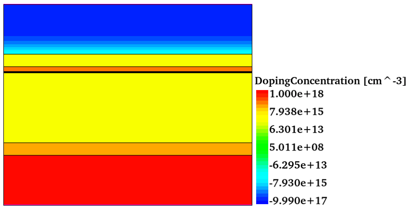
Figure 1 InGaAs-InP APD Detector Sde Simulation Structure
Introduction to InGaAs-InP APD Detectors and Electrical Simulation
Under dark conditions, due to the absence of photon-generated carriers, the current is relatively low and is mainly caused by thermally generated carriers. The current includes dark current generated by thermal excitation, and the current follows a square non-linear relationship with reverse bias. When the voltage exceeds the breakdown voltage, the dark current is also amplified by the multiplication effect, but because there are no photon-generated carriers, the current level is relatively low but increases rapidly.
Under illumination, the increase in photon-generated carriers affects the width of the space charge region, which in turn affects the capacitance. Typically, in the low-voltage region, the CV curve may show dynamic changes. In the high-voltage region, the avalanche multiplication effect and changes in the depletion region may cause the capacitance to change with increasing voltage. However, the specific impact of illumination on the capacitance in this region is more complex and requires material property analysis. Under dark conditions, the capacitance of the APD follows a typical pn-junction capacitance characteristic, where as the reverse bias increases, the depletion region expands and the capacitance decreases. As the reverse voltage approaches the breakdown voltage, the capacitance of the APD still changes with further increases in reverse voltage, but because there are no photon-generated carriers, the change is mainly caused by the strengthening of the electric field and the expansion of the depletion region.
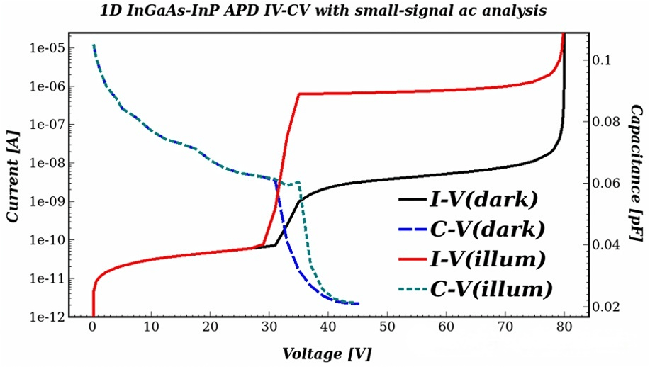
Figure 2: InGaAs-InP APD Detector I-V and C-V Simulation Characteristics under Dark and Illumination Conditions
In the simulation and characterization of InGaAs-InP APD (Avalanche Photodiode) devices, some specific parameters can be extracted using Svisual, such as Vb_dark, Vp_dark, jp_dark, Vb_illum, Vp_illum, and jp_illum. These parameters represent the different characteristics of the device under dark (no illumination) and illuminated (with illumination) conditions. The parameter Vb_dark (Dark Breakdown Voltage) is the breakdown voltage of the device under no illumination, indicating the voltage at which avalanche breakdown occurs in the APD without incident light. Understanding this parameter helps determine the working voltage range of the APD to ensure it does not enter avalanche breakdown during normal operation. The parameter Vp_dark (Dark Punch-Through Voltage) is the punch-through voltage of the device under dark conditions, indicating the voltage at which significant carrier migration begins between the absorption layer and the multiplication layer without photons. This parameter helps designers determine the voltage control range to avoid operating below the punch-through voltage, which can affect performance. The parameter jp_dark (Dark Current Density) is the dark current density under no illumination, which is the current density through the device under dark conditions. Typically, dark current should be kept as low as possible because high dark current increases noise and reduces sensitivity. Dark current density is an important parameter in the performance of the APD, affecting its detection ability at low light signal intensities. The parameter Vb_illum (Illuminated Breakdown Voltage) is the breakdown voltage of the device under illumination, indicating the voltage at which avalanche breakdown occurs under incident light. The breakdown voltage under illumination typically differs from that under dark conditions because photon-generated carriers affect the avalanche process. Vp_illum (Illuminated Punch-Through Voltage) is the punch-through voltage of the device under illumination. With incident light, photon-generated carriers fill the absorption layer and migrate to the multiplication layer, causing changes in the electric field and carrier distribution. Therefore, the punch-through voltage under illumination is also a key parameter that should be considered when evaluating and designing the device. jp_illum (Illuminated Current Density) is the current density of the device under illumination. The current density under illumination reflects the impact of incident light intensity and the device’s gain on the current. A high-quality APD should exhibit a high current density response under illumination, indicating high photon sensitivity and signal gain.
The extracted results from Svisual are Vb_dark=79.98V, Vp_dark=38.06V, jp_dark=1.813e-9 A/cm², Vb_illum=79.58V, Vp_illum=39.24V, jp_illum=6.409e-7 A/cm².
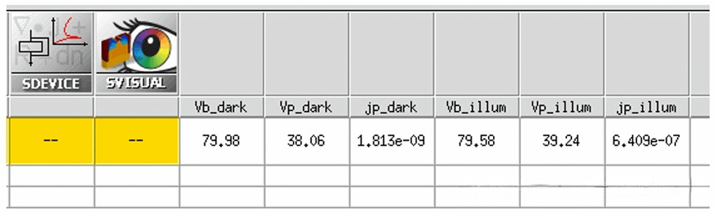
Figure 3: InGaAs-InP APD Detector Simulation Parameter Extraction Results
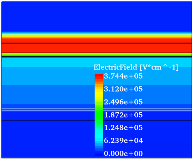
Figure 4 : Electric Field Distribution of InGaAs-InP APD Detector at Reverse Bias 50V