


Avalanche photodiodes (APDs) represent a significant advancement in photodetection technology, offering high sensitivity and internal gain mechanisms that make them invaluable for applications requiring detection of weak light signals.
I. Introduction to Avalanche Photodiodes
Avalanche photodiodes are highly sensitive semiconductor devices that convert light into electrical signals through the photovoltaic effect. Unlike conventional photodiodes, APDs are designed to operate with high reverse bias voltages that approach breakdown voltage, enabling internal multiplication of photocurrent through avalanche breakdown effects. This internal gain mechanism allows APDs to detect relatively small amounts of light with significantly improved signal-to-noise ratios compared to standard photodiodes.
Historically, the avalanche photodiode was invented by Japanese engineer Jun-ichi Nishizawa in 1952. Since then, APDs have evolved substantially, with numerous advancements in materials, structures, and applications. From a functional perspective, APDs can be considered the semiconductor analog of photomultiplier tubes, although they operate on different physical principles.
When compared to other photodetection technologies such as photomultiplier tubes (PMTs), APDs offer several advantages. They are less sensitive to magnetic fields, provide higher quantum efficiency for input light signals, and require lower operating voltages. Additionally, APDs typically exhibit greater durability and lower cost compared to tube-based alternatives.
II. Operating Principles
The Avalanche Effect
The fundamental operating principle of APDs involves a process called impact ionization, which creates an avalanche multiplication effect. When a photon with sufficient energy (greater than the semiconductor’s bandgap) is absorbed by the APD, it generates an electron-hole pair. Under high reverse bias voltage, these carriers are strongly accelerated in the resulting intense electric field within the device.
As these accelerated carriers move through the semiconductor material, they gain sufficient kinetic energy to collide with atoms in the crystal lattice, creating additional electron-hole pairs through a process called impact ionization. These newly generated carriers are similarly accelerated and create even more carriers, resulting in a chain reaction or “avalanche” of carrier generation.
This multiplication process effectively amplifies the original photocurrent, significantly enhancing the device’s sensitivity to light. The avalanche multiplication can be represented mathematically using the multiplication factor (M), which increases exponentially with the applied reverse voltage.
Reverse Bias and Breakdown
APDs operate under high reverse bias conditions, typically tens or even hundreds of volts, depending on the device design and materials. This reverse bias creates a strong electric field across the device’s junction, which is crucial for the avalanche process to occur.
The applied voltage is typically maintained just below the breakdown voltage of the device for normal APD operation. As the reverse voltage approaches the breakdown threshold, the multiplication factor increases significantly, allowing for higher sensitivity. However, operating too close to breakdown can lead to excessive noise and potential device damage.
III. Structure and Design
Basic Structure
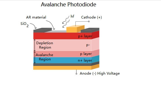
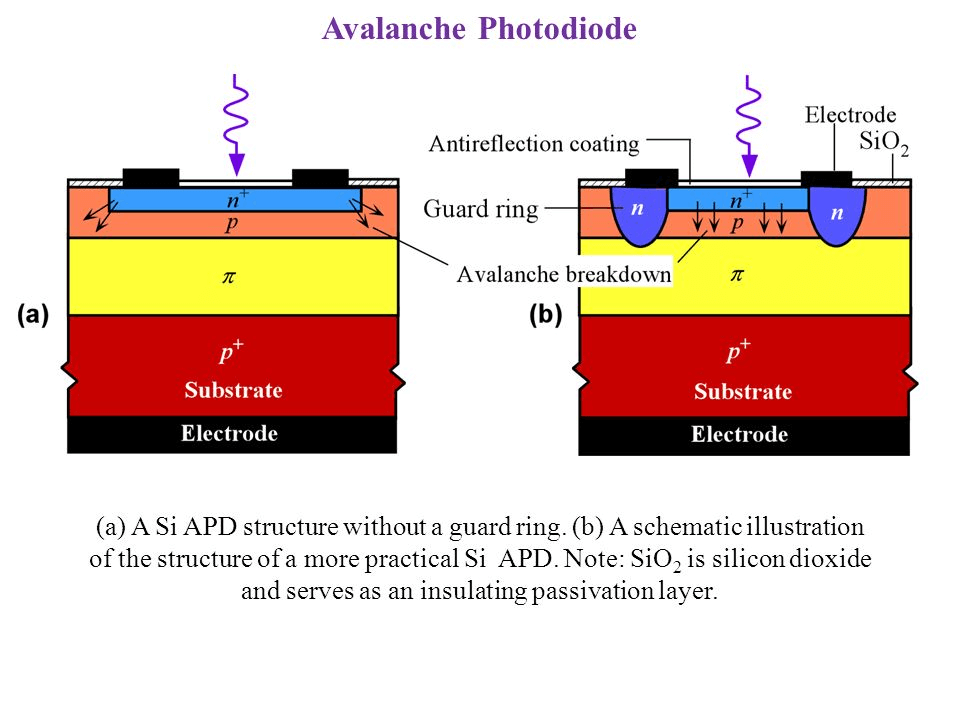
The structure of an avalanche photodiode typically resembles that of a PIN photodiode but with modifications to optimize the avalanche effect. A common APD structure consists of two heavily doped regions (P+ and N+) and two lightly doped regions (I and P). The intrinsic (I) region serves as the primary absorption region for incoming photons, while a thin, high-field region near the junction serves as the avalanche multiplication region.
The depletion layer width in an APD is typically thinner than in PIN photodiodes, which enhances the electric field strength necessary for avalanche multiplication[2]. The P+ region functions as the anode, while the N+ region serves as the cathode.
Structural Variations
Different APD designs exist to optimize performance for specific applications or wavelength ranges. One key structural variation is the choice between P-incidence and N-incidence structures:
P-incidence structure: In this design, light enters through the P-side of the device. This structure is particularly advantageous for short-wavelength light detection, as the generated carriers from light incidents near the surface enter the avalanche layer with 100% certainty, maximizing the avalanche effect.
N-incidence structure: This more common design has light entering through the N-side. However, with short-wavelength light, carriers may be generated before reaching the avalanche layer, reducing sensitivity.
Additionally, various edge terminations have been developed for APDs to enhance breakdown voltage control and device reliability. These include ion implanted edge termination, bevel etch edge termination, deep etch edge termination, field plate edge termination, and moat etch edge termination.
IV. Key Characteristics
Responsivity and Gain
One of the most significant advantages of APDs is their high responsivity due to the internal gain mechanism. The responsivity of an APD is substantially higher than that of standard PIN photodiodes. The current amplification process strongly increases the responsivity, with the multiplication factor (M) typically ranging from 50 to 1000 for silicon APDs and 10 to 40 for InGaAs and germanium APDs.
It’s important to note that the gain depends strongly on the reverse voltage and may vary substantially between devices. Manufacturers typically specify a voltage range within which all devices reach a certain responsivity. Recent advancements have achieved extraordinarily high gains, with some research demonstrating gain values up to 5.9 × 10^5 in specialized APD designs.
Quantum Efficiency
Despite their high responsivity, the quantum efficiency of APDs is not necessarily higher than other photodiodes – it remains below 100% and can sometimes be lower than standard photodiodes. This means that not all incident photons contribute to the photocurrent, even though those that do create a much stronger signal through the avalanche effect.
Noise Characteristics
The noise characteristics of APDs are complex and critical to their performance. The total noise in APDs includes contributions from several sources:
- Shot Noise: Results from the discrete nature of charge carriers and increases with photocurrent. It is influenced by both the primary photocurrent and the multiplied current due to avalanche gain.
- Dark Current Noise: Originates from leakage current within the APD, present even without incident light. Dark current can be divided into “bulk” leakage (thermal generation or tunneling) and “surface” leakage components.
- Multiplication Noise: Also called excess noise, this results from statistical fluctuations in the avalanche process. The excess noise factor (F) increases with higher gain[10].
The noise performance of APDs is characterized by the excess noise factor, which quantifies how much the electronic noise power increases compared to an ideal photodetector. This factor depends on the applied voltage, material properties (particularly the ionization coefficient ratio), and device design.
Despite these noise sources, APDs can provide better overall noise performance than PIN photodiodes when electronic noise is a limiting factor. This is because the large responsivity helps reduce the impact of electronic noise from subsequent amplification stages.
Detection Bandwidth
APDs can achieve high detection bandwidths, making them suitable for high-speed applications. Recent advancements have demonstrated bandwidths up to 53 GHz in specialized designs. However, there is an inherent trade-off between bandwidth and amplification factor – higher gain typically results in lower bandwidth due to increased transit time through the avalanche region.
The detection bandwidth is limited by several factors, including:
- CR time constant: Determined by the junction capacitance and load resistance
- Drift time: The time required for carriers to move through the depletion layer
- Multiplication time: The time required for carriers to pass through the avalanche layer, which increases with gain
V. Materials and Wavelength Ranges
Different semiconductor materials are used in APDs to target specific wavelength ranges:
Silicon-Based APDs
Silicon-based APDs are sensitive in the wavelength region from approximately 450 to 1000 nm (sometimes up to 1100 nm), with maximum responsivity occurring around 600-800 nm. These APDs can achieve high multiplication factors between 50 and 1000, making them suitable for visible light detection applications.
InGaAs and Germanium APDs
For longer wavelengths up to approximately 1.7 μm, APDs based on germanium or indium gallium arsenide (InGaAs) are employed. InGaAs APDs, while more expensive than germanium-based devices, offer superior noise performance and higher detection bandwidth. Their high absorption coefficient allows for a thinner absorbing layer, which contributes to better performance characteristics.
Another approach involves germanium/silicon (GeSi) hybrid devices, where radiation is absorbed in germanium, and carriers are transferred into a silicon region for charge multiplication.
GaN-Based APDs for UV Detection
Gallium nitride (GaN) is used for APDs designed to detect ultraviolet light. GaN-based APDs are naturally suited for applications requiring high-temperature or harsh environment tolerance. They have enabled significant advances in UV detection, offering durability and performance advantages over traditional UV detectors based on photomultiplier tubes.
Design considerations for GaN APDs include:
- Light doping density (LDD) in the epitaxial layers to provide sufficient distance for carriers to establish an avalanche process
- Optimized edge termination to eliminate localized peak electric fields around device edges
GaN APDs exhibit a positive temperature coefficient of breakdown voltage, meaning the breakdown voltage increases with temperature. This characteristic makes them more stable at elevated temperatures compared to other semiconductor materials.
Other Materials
Less common semiconductor materials used in specialized APD applications include:
- HgCdTe for mid-infrared detection up to wavelengths of approximately 14 μm (used under cryogenic conditions)
- Ga₂O₃-based APDs for solar-blind detection, with recent research showing record-high avalanche gain
VI. Advanced Concepts and Recent Developments
Geiger Mode Operation
If exceptionally high gain (10^5 to 10^6) is required, APDs can be operated in “Geiger mode,” where the reverse voltage is set above the breakdown voltage. In this mode, the device is also known as a Single-Photon Avalanche Diode (SPAD).
When operating in Geiger mode, the photodetector requires current-limiting and quick-quenching techniques to control the avalanche process. Active and passive current-quenching approaches have been developed for this purpose. This mode is particularly valuable for single-photon detection applications, provided that dark count rates and afterpulsing probability remain sufficiently low.
Recent Research Breakthroughs
Recent advances in APD technology include:
- Ultra-high gain-bandwidth products: Researchers have implemented a germanium/silicon APD with a gain-bandwidth product exceeding 1 THz. This breakthrough was achieved by precisely shaping the electric field distribution and engineering the resonant effect in the avalanche process.
- Enhanced solar-blind detection: New unipolar barrier designs have demonstrated record-high avalanche gain up to 5.9 × 10^5 and detectivity of 2.33 × 10^16 Jones among wafer-scale ultraviolet APDs.
- Improved breakdown voltage control: Novel approaches to controlling breakdown voltage include the incorporation of diffusion sinks formed simultaneously with the device region of the APD.
These advancements continue to push the boundaries of what’s possible with APD technology, enabling new applications and improved performance in existing ones.
Applications
Avalanche photodiodes find use in numerous applications that require high-sensitivity light detection:
Optical Fiber Communications
APDs are widely used in optical fiber communication systems, where they convert optical signals into electrical signals with high sensitivity and speed. Their internal gain allows for detection of weak optical signals over long transmission distances, making them ideal for telecommunications infrastructure.
LiDAR and Rangefinding
The high sensitivity and fast response time of APDs make them excellent detectors for laser rangefinding and LiDAR (Light Detection and Ranging) applications. These technologies are critical for autonomous vehicles, 3D mapping, and various industrial and military applications requiring precise distance measurement.
Medical Imaging
APDs are employed in medical imaging technologies, particularly those requiring detection of low light levels, such as positron emission tomography (PET). Their high sensitivity enables better image quality with lower radiation doses in certain applications.
Scientific Research and Instrumentation
In scientific research, APDs are used in various instruments that require sensitive light detection, including:
- Optical time-domain reflectometers (OTDRs) for fiber optic network testing
- High-speed laser scanners and laser microscopy
- Particle physics research
- Quantum optics and quantum key distribution systems
Additional Applications
Other notable applications include:
- UV detection for flame sensing, chemical detection, and security applications
- X-ray and gamma-ray scintillation detection when coupled with appropriate scintillator materials
- Environmental monitoring and sensing
- Astronomy and space-based observation systems
VII. Conclusion
Avalanche photodiodes represent a critical technology in modern optoelectronics, bridging the gap between conventional photodiodes and photomultiplier tubes. Their ability to provide internal gain through the avalanche effect enables high-sensitivity detection while maintaining the robustness and compactness of semiconductor devices.
The continuing evolution of APD technology, including advances in materials, structural designs, and operating modes, continues to expand their capabilities and application range. Recent breakthroughs in gain-bandwidth products, specialized designs for particular wavelength ranges, and improvements in noise characteristics are pushing the boundaries of what’s possible with these devices.
As research progresses, we can expect further refinements in APD technology, particularly in areas such as reduced noise, increased bandwidth, enhanced sensitivity, and expanded wavelength coverage. These developments will continue to make APDs indispensable components in both established fields like telecommunications and emerging areas such as quantum technologies, autonomous systems, and advanced scientific instrumentation.