
It is applied in autonomous driving field.
Autonomous Driving
Deep Space Exploration
Gravity Potential Measurement
...
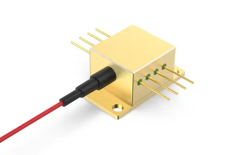
InGaAs Avalanche Photodiode
Optical fiber sensing
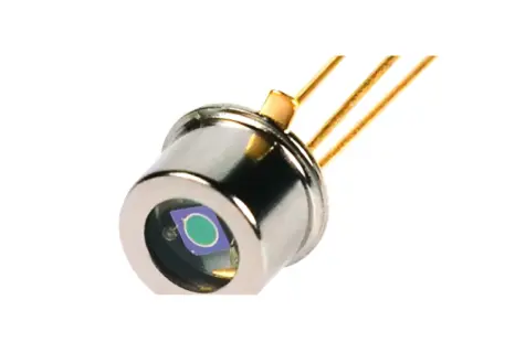
InGaAs Negative Feedback Avalanche Photodiode
High speed fiber optic communication
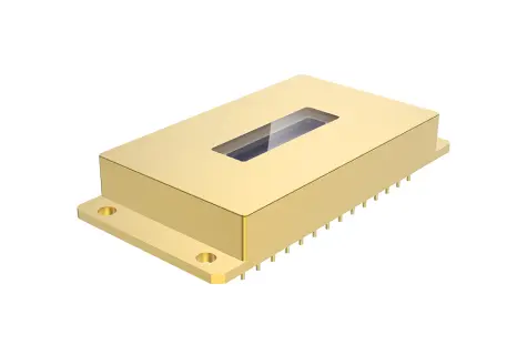
InGaAs Small Panel Linear Array Focal Plane Detector
Detection of agricultural products
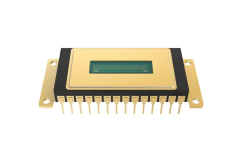
InGaAs Large Panel Linear Array Focal Plane Detector
Foreign body screening
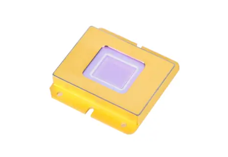
InGaAs Arrayfocalplane sensor
GD-NIR32030M
Photodiode module
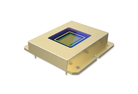
InGaAs Array Focal Plane Sensor
GD-NIR64015M
Photodiode module
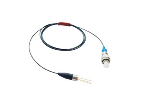
OP300D InGaAs Geiger Mode Avalanche Photodiode
Photodiode module
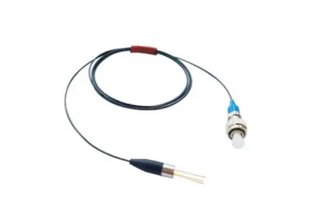
OP301D InGaAs Geiger Mode Negative Feedback Avalanc...
Photodiode module
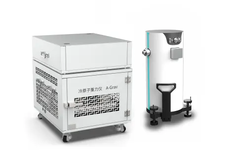
Cold Atomic Gravimeter
Provide gravity reference values
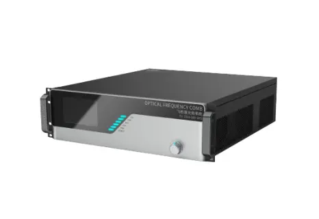
Femtosecond Laser Frequency Comb
High-resolution spectroscopy

Single Photon Ranging System
Mobile target monitoring
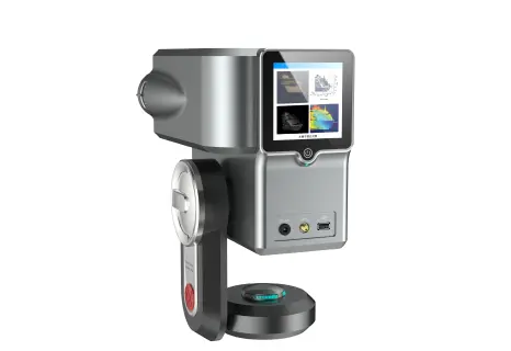
Single Photon Imaging System
Counter terrorism operations
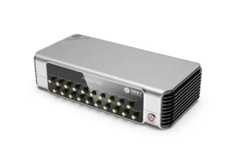
Time-to-Digital Converter
LiDAR, Single Photon Imaging


Utilize quantum states to encode information, ensuring communication security.

Employ optical principles to detect environmental parameters via light signals for monitoring and control purposes.

Using laser pulses to calculate distances enables precise measurements and positioning.

Use light signals to capture images of internal biological structures and functions for medical applications.
Explore the diverse applications of our products and discover the exceptional innovation and significant benefits they will bring to your industry.

Ultra High-Speed Encoding

Agricultural Product Testing

Solar Panel Silicon Wafer Inspection
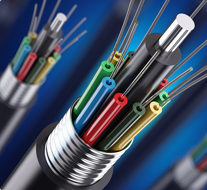
ROF System

Manufacturing Support System
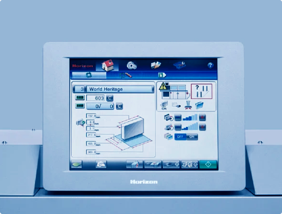
Photometry System

Life Science & Medical Systems

Semiconductor Manufacturing

Text 1

Text 2

Text 3

Text 4

Text 5

Text 6

Text 7

Text 8
Download catalogs, technical information, application notes, and product datasheets here.
Why Choose Us
Learn more about our comprehensive product solutions, we’re confident we can offer you the best options.

We are a dedicated company specializing in the field of optoelectronics.

Ensure that customers receive personalized solutions that fully meet their needs.

Many products are industry-leading in terms of performance and functionality.


We are a dedicated company specializing in the field of optoelectronics. Our expertise shines through in every facet of our work.

Our expertise in customization ensures that each client receives a personalized solution that perfectly suits your needs.

Based on our company’s research and development capabilities, many of our products are industry-leading in terms of performance and functionality.