


2. Basic Concepts of Single-Photon Avalanche Diodes (SPADs)
To fully appreciate the engineering achievements of the OP430D, one must first understand the underlying physics and performance metrics of SPAD technology. A SPAD is essentially a p-n junction diode specifically designed to be biased well above its reverse breakdown voltage ( Vᵦᵣ ), a regime known as Geiger mode.
2.1 The Geiger Mode Mechanism
In a standard Avalanche Photodiode (APD) operating in linear mode, the reverse bias is kept just below the breakdown voltage. An absorbed photon creates an electron-hole pair, which is accelerated by the electric field to create secondary pairs via impact ionization. This results in a finite gain ( M), typically between 10 and 100, where the output current is proportional to the input light intensity.
In contrast, a SPAD operates with an “excess bias” ( Vₑₓ) above the breakdown voltage. In this metastable state, the electric field is so high (typicallyV/cm) that a single charge carrier—generated by the absorption of a photon—can trigger a self-sustaining runaway avalanche of impact ionizations. The gain effectively becomes infinite (10^5 to 10^6), and the diode becomes a binary switch: it is either “off” (waiting for a photon) or “on” (conducting a macroscopic current). This macroscopic current pulse is independent of the number of photons that triggered it; a single photon triggers the same avalanche as multiple simultaneous photons. Therefore, the device counts events, not intensity.
2.2 Key Performance Metrics
The utility of a SPAD is defined by four critical parameters, all of which are interrelated and involve inherent trade-offs:
1. Photon Detection Efficiency (PDE)
This is the probability that a single photon incident on the detector will successfully trigger a detectable avalanche. PDE is the product of the quantum efficiency (probability of absorption) and the avalanche triggering probability (probability that the carrier initiates a breakdown). For InGaAs SPADs like the OP430D, PDE is heavily dependent on the excess bias voltage; higher voltage increases the probability of an avalanche but also increases noise.
2. Dark Count Rate (DCR)
Even in total darkness, a SPAD will occasionally fire. These “dark counts” are caused by thermally generated carriers (electrons/holes) or carriers tunneling through the bandgap. In InGaAs, which has a smaller bandgap than Silicon, thermal generation is a major noise source, necessitating deep cooling. DCR is the primary noise floor of the detector and is measured in Hertz (counts per second)
3. Afterpulsing
This is a noise phenomenon specific to SPADs. During an avalanche, millions of charge carriers flow through the high-field region. Some of these carriers can become trapped in crystal defects (traps) within the semiconductor lattice. If these trapped carriers are released after the avalanche has been quenched and the voltage restored to Geiger mode, they can trigger a second, spurious avalanche correlated with the first. This is called an “afterpulse.” Reducing afterpulsing requires high material purity and the imposition of a “dead time” to allow traps to empty.
4. Timing Jitter
This refers to the variation in the time delay between the arrival of the photon and the onset of the electrical output pulse. Low jitter is crucial for “Time-of-Flight” (ToF) applications like LiDAR, where distance is calculated based on the photon’s travel time. InGaAs SPADs typically exhibit jitter in the range of 100-300 picoseconds.
2.3 Quenching Circuits
Because the avalanche in Geiger mode is self-sustaining, it must be actively stopped (quenched) to prevent the device from overheating and to reset it for the next photon.
- Passive Quenching: A large series resistor drops the bias voltage when current flows, stopping the avalanche. This is simple but leads to long recovery times.
- Active Quenching: An external circuit detects the avalanche onset and actively lowers the bias voltage, then restores it after a set hold-off time.
- Gated Quenching: The detector is only biased above breakdown for a short window (gate) when a photon is expected. This is the standard mode for InGaAs SPADs in QKD to minimize noise.
3. Working Principles of the OP430D
The OP430D is built upon the foundational physics of InGaAs/InP heterostructures, engineered to overcome the limitations of bulk Germanium detectors that were previously used for infrared detection.
3.1 Separate Absorption, Grading, Charge, and Multiplication (SAGCM) Structure
The OP430D utilizes a complex vertical semiconductor stack known as SAGCM to optimize performance:
Absorption Region (InGaAs)
The topmost active layer is Indium Gallium Arsenide (In₀.₅₃Ga₀.₄₇As).This alloy composition is lattice-matched to Indium Phosphide (InP) substrates and possesses a bandgap of 0.75 eV, allowing it to efficiently absorb photons up to 1700 nm. However, InGaAs has a relatively high tunneling current if subjected to high electric fields.
Multiplication Region (InP):
To avoid high tunneling noise in the InGaAs layer, the avalanche multiplication process is confined to a separate Indium Phosphide (InP) layer. InP has a wider bandgap (1.35 eV) and can withstand the high electric fields necessary for impact ionization without excessive tunneling noise.
Grading Layer (InGaAsP):
A crucial “grading” layer of Indium Gallium Arsenide Phosphide is placed between the InGaAs absorption layer and the InP multiplication layer. Without this, the sharp discontinuity in the valence band between InGaAs and InP would trap photogenerated holes, preventing them from entering the multiplication region and causing a “slow tail” in the timing response (high jitter). The grading layer smooths this transition, allowing holes to flow freely.
Charge Layer:
A thin, highly doped charge layer is inserted to shape the electric field profile, ensuring the field is high in the InP layer (for multiplication) but low in the InGaAs layer (to prevent tunneling).
3.2 Thermal Environment Control
The OP430D integrates a three-stage Thermoelectric Cooler (TEC) directly into the butterfly package. This is a critical working principle because the performance of InGaAs SPADs is exponentially dependent on temperature.
Dark Count Suppression:
The dark count rate in InGaAs typically halves for every 10°C reduction in temperature. By cooling the chip to -40°C or -50°C (as permitted by the OP430D’s 11.9V/0.8A TEC), the module suppresses thermally generated carriers, reducing DCR from hundreds of kilohertz (at room temperature) to just a few kilohertz.
Breakdown Voltage Stability:
The breakdown voltage (Vᵦᵣ) of the device shifts with temperature (coefficient η≈0.15V/°C). 2 Precise temperature control is required to maintain a constant “excess bias” (VEX=VBIAS−VBR). If the temperature drifts, Vᵦᵣ changes, and the effective overvoltage (and thus PDE) fluctuates, destabilizing the system. The integrated thermistor (10 kΩ NTC) and TEC loop ensure this stability.
3.3 The Advantages of Dual-Channel Architecture
The “D” in OP430D stands for Dual-Channel. This architecture, where two SPAD chips are co-packaged, offers distinct advantages over single-channel modules:
Common Mode Rejection:
In gated operation, the rapid voltage transitions of the gate pulse inject a capacitive “spike” into the output signal, which can mask the small avalanche current. By using two identical SPADs (one active, one as a reference, or both active in a differential pair), readout circuits can subtract the common capacitive response, leaving only the avalanche signal. This technique, known as “self-differencing” or “balanced detection,” allows for the detection of smaller avalanches, which in turn reduces the charge flow per event and minimizes afterpulsing.
Synchronization:
Since both detectors sit on the same thermal stage, they experience identical temperature environments. This ensures their breakdown voltages track together, simplifying the biasing electronics for multi-channel QKD systems where maintaining channel balance is critical.
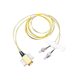
4. Technical Characteristics of the OP430D
Based on the official datasheet, the OP430D exhibits a set of specifications that position it as a high-performance component for demanding applications. These characteristics are divided into “Linear Mode” (characterizing the diode junction) and “Geiger Mode” (characterizing the photon counting performance).
4.1 Absolute Maximum Ratings and Operating Conditions
Before examining performance, it is vital to understand the operational limits to ensure device longevity.
Operating Temperature
The module is rated for ambient temperatures from -50°C to +60°C. However, the internal APD chip is recommended to operate between -50°C and -30°C using the TEC.
TEC Specifications
The robust three-stage cooler requires up to 11.9 V and 0.8 A. This indicates a high cooling capacity (ΔT), likely capable of achieving a 60-70°C differential from the case temperature.
Optical Power
The maximum continuous input optical power is 1 mW. Exceeding this can cause catastrophic damage to the small active area due to high current density.
Reverse Bias
The absolute maximum reverse DC bias is VBR+5V. This sets a hard limit on the “excess bias” one can apply. Since PDE increases with excess bias, this effectively caps the maximum achievable efficiency to protect the device from dielectric breakdown or thermal runaway.
4.2 Linear Mode Parameters (at 25°C)
These parameters are measured before the device enters Geiger mode and serve as a baseline for quality control.
Active Area
The effective detection surface diameter is 25μm. This small size is standard for high-speed SPADs, as it minimizes capacitance (listed aspF) and dark counts (which scale with area).
Breakdown Voltage (Vᵦᵣ):
Ranges from 60 V to 85 V. This wide manufacturing tolerance is typical for InGaAs APDs; however, the dual-channel nature implies that the two diodes within a single package are likely “binned” or matched to have very similarvalues.
Dark Current
In linear mode (atVBR−1V), the dark current is ≤1nA. This is an excellent figure of merit, indicating high material quality and low defect density at the surface and bulk of the semiconductor.
Responsivity
A/W at 1550 nm. This confirms the high quantum efficiency of the InGaAs absorption layer.
4.3 Geiger Mode Parameters (at -40°C)
These are the critical figures for single-photon applications.
Photon Detection Efficiency (PDE)
The datasheet lists a “Minimal” PDE of 3%, but crucially, the Dark Count Rate is tested at a condition of SPDE = 20%. This implies the device is designed and qualified to operate at 20% efficiency. The 3% figure likely represents a conservative baseline at very low excess bias, while 20% is the standard operating point for most applications like QKD.
Dark Count Rate (DCR)
kHz (at 20% PDE). This is a competitive specification. Early generations of InGaAs SPADs struggled with DCRs in the 10-50 kHz range. Achieving 2.5 kHz allows for a significantly higher Signal-to-Noise Ratio (SNR), extending the range of QKD links and the sensitivity of LiDAR systems.
Afterpulsing (APP)
(at 10% PDE, 500 ns hold-off). This is a critical parameter. A 4% afterpulse probability means that for every 100 true photons detected, 4 false “ghost” detections will occur. The 500 ns dead time condition suggests the trap lifetimes are reasonably short, allowing for detection rates in the MHz range.
Timing Jitter
ps. While adequate for many applications, this is slightly higher than the <100 ps jitter seen in some ultra-fast research devices. However, 300 ps corresponds to a spatial resolution of roughly 4.5 cm in LiDAR (two-way travel), which is sufficient for many mapping and obstacle detection tasks.
5. Comparison with Mainstream Brands
The market for InGaAs SPADs is niche and highly specialized. The OP430D competes in a landscape defined by a few major players: Wooriro (Korea), Hamamatsu (Japan), Excelitas (USA/Canada), and system-level integrators like ID Quantique (Switzerland).
| Feature | Lonten OP430D | Wooriro SPD6524Q | Hamamatsu G14858 | Excelitas C30733 |
|---|---|---|---|---|
| Configuration | Dual-ChannelModule | Dual-ChannelModule | SingleAPD Component | SingleAPD Component |
| Package | 14-pin Butterfly + 3-Stage TEC | 14-pin Butterfly + 3-Stage TEC | TO-18 (Metal Can) | TO-18 / Fiber Pigtail |
| Active Area | 25um | 25um | 200um (Typical) | 30um |
| Op. Mode | Optimized forGeiger Mode | Optimized forGeiger Mode | Linear (can do Geiger) | Linear (can do Geiger) |
| PDE (1550nm) | ~20% (Typ. inferred) | ≥10% (Min) | N/A (Linear Spec) | N/A (Linear Spec) |
| DCR | ≤2.5 kHz (@ -40°C) | ≤2.5 kHz (@ -30°C) | 50 nA (Dark Current) | 0.5 nA (Dark Current) |
| Target Use | QKD, LiDAR, R&D | QKD, LiDAR, OTDR | OTDR, Rangefinding | OTDR, High-Speed Rx |
5.1 Analysis vs. Wooriro (The Direct Rival)
The Wooriro SPD6524Q 12 is the most direct competitor to the OP430D. Both utilize the same 14-pin butterfly form factor, both integrate 3-stage TECs, and both offer dual-channel configurations. Their specifications are strikingly similar: 25active area, DCR around 2.5 kHz, and similar spectral ranges.
Strategic Insight: The similarity suggests both companies are targeting the exact same standardized footprint for QKD system integrators. The choice between them often comes down to supply chain availability, pricing, and specific batch consistency (binning precision) rather than fundamental architectural differences. Wooriro is a well-established player in passive optical components (PLC splitters), giving them strong packaging heritage.14 Lonten’s focus appears more aggressively tuned towards the quantum sensing market specifically.
5.2 Analysis vs. Hamamatsu (The Industry Benchmark)
Hamamatsu Photonics is the behemoth of the industry. Their products, such as the G14858 or G8931 series 15, are typically sold as discrete TO-can components or as fully instrumented modules (e.g., C16531) that include the readout electronics.
Differentiation: Hamamatsu does not prominently market a “dual-channel raw butterfly module” like the OP430D. They sell the chip (requiring the user to build the cooling and packaging) or the instrument (complete with power supply and logic). The OP430D occupies the “middle ground”—a packaged, cooled, fiber-coupled component that is ready for integration but allows the user to design their own custom quenching electronics. This is highly attractive for QKD researchers who need control over the gating circuit but don’t want to wire-bond raw chips.
5.3 Analysis vs. Excelitas (The Volume Leader)
Excelitas (formerly PerkinElmer) is famous for its Silicon SPCM modules. In the InGaAs domain, their C30645 and C30733 series are dominant in high-volume linear applications like OTDR (Optical Time Domain Reflectometry) and range-finding.
Differentiation: Excelitas datasheets focus heavily on Noise Equivalent Power (NEP), Bandwidth, and Responsivity—metrics for linear analog detection. While their chips can operate in Geiger mode, the OP430D is characterized for it (specifying jitter, APP, and DCR directly). For a user building a single-photon counter, the OP430D datasheet provides the relevant guarantee, whereas using a linear APD requires “off-label” characterization by the user.
5.4 Analysis vs. ID Quantique (The System Integrator)
ID Quantique (IDQ) produces the ID230, a fully turnkey detection system.
Relationship: IDQ is effectively a potential customer for a product like the OP430D. The ID230 is a box you plug into a wall; the OP430D is a component you solder onto a PCB. The OP430D allows OEMs to build systems competing with the ID230 at a fraction of the cost, provided they have the engineering capability to design the control electronics.
6. Technology Trends and Future Outlook
The OP430D represents the mature, reliable state of the art for 2024-2025. However, the field is evolving rapidly, driven by the intense demands of the quantum internet and autonomous vehicle perception.
6.1 Scaling to Arrays: From 2 to 1024 Pixels
While the dual-channel OP430D is excellent for balanced detection, the industry is moving toward imaging arrays. Lonten is already developing 4×4 (OP501C) and 8×8 (OP520C) InGaAs SPAD arrays. The future lies in 32×32 and 64×64 focal plane arrays (FPAs) for “Flash LiDAR,” where an entire scene is captured in a single laser pulse without mechanical scanning. The challenge will shift from detector physics to readout integrated circuit (ROIC) design—handling the massive data throughput and thermal load of thousands of SPADs firing simultaneously.
6.2 Hybrid Integration and Photonic Circuits
Current QKD systems use bulky fiber components. The trend for 2025 is Hybrid Integration, where InGaAs SPAD chips are flip-chip bonded directly onto Silicon Photonics or Silica-on-Silicon waveguides.8 This “QKD on a chip” approach eliminates the butterfly package entirely, shrinking a server-rack sized system down to a transceiver card. While the OP430D is the solution for today’s rack-mounted systems, its successor might be a bare die designed for waveguide coupling.
6.3 Negative Feedback Avalanche Diodes (NFADs)
The OP430D requires external quenching. The next technological leap is the NFAD, where a thin-film quenching resistor is monolithically integrated directly on top of the SPAD pixel.20 This minimizes parasitic capacitance to femto-farad levels, enabling faster quenching, lower afterpulsing, and sharper timing resolution. Future iterations of Lonten’s product line will likely incorporate NFAD structures to push performance limits further.
6.4 The Challenge of Superconducting Detectors (SNSPDs)
Superconducting Nanowire Single-Photon Detectors (SNSPDs) offer performance that InGaAs cannot match: >90% efficiency, near-zero dark counts (<10 Hz), and <20 ps jitter.22 However, they require cryogenics (2-4 Kelvin). The market is bifurcating: SNSPDs will dominate high-end laboratory quantum computing, while InGaAs SPADs like the OP430D will own the “deployable” market—telecom closets, satellites, and vehicles—where liquid helium cooling is impossible. The OP430D’s ability to perform adequately at -40°C (achievable with a simple TEC) is its greatest strategic asset against the superconducting threat.
7. Conclusion
The OP430D Dual Channel InGaAs SPAD Detector serves as a vital enabler for the SWIR photon-counting ecosystem. By packaging two matched, high-performance sensors into a thermally stabilized, industry-standard butterfly module, Lonten has created a versatile “building block” for advanced optical systems.
Its specifications—particularly a manageable 2.5 kHz Dark Count Rate at 20% efficiency—strike a pragmatic balance between sensitivity and noise, making it suitable for the rigorous demands of Quantum Key Distribution and the high-speed requirements of eye-safe LiDAR. While it faces stiff competition from Wooriro’s nearly identical offerings and the broad portfolios of Hamamatsu and Excelitas, the OP430D’s specific focus on Geiger-mode characterization and dual-channel integration gives it a distinct value proposition for OEMs seeking to build balanced, differential detection systems.
As the industry marches toward large-format arrays and integrated photonic circuits, the OP430D stands as a mature, robust solution for the current generation of deployable quantum and sensing technologies, bridging the gap between scientific possibility and industrial reality.